Putting on the Board
FIRs on Boards
Please Log In for full access to the web site.
Note that this link will take you to an external site (https://shimmer.mit.edu) to authenticate, and then you will be redirected back to this page.
The Goal
OK this build is going to have a lot of moving parts. The big picture is you're going to build a real-time FIR-filter that does sweet, controllable (from Python) one-line convolution on video feeds from any regular computer with a monitor output.
You should be able to start from either Week 2's project (if you want), or you can just start a new Zynq 7000 (Pynq) project from scratch. I didn't do that personally, I instead made a new project, but there's nothing we're doing here that should inherently cause any issues as far as I can tell. We're going to be making a new piece of MMIO-IP but multiples of those can co-exist in the same project because they'll be placed into different regions in the system's overall address space.
Regardless, having a project with a Zynq processor system set up the same way we did in Week 2 is a must for this project. Make sure you're starting there. Whether or not you have the SPI controller orthogonal to the problem at hand.
The XDC needs to be slightly modified from before. Either start with the base.xdc or make sure the one you're using has the following lines uncommented in it:
## Clock signal 125 MHz
set_property -dict { PACKAGE_PIN H16   IOSTANDARD LVCMOS33 } [get_ports { sysclk }]; #IO_L13P_T2_MRCC_35 Sch=sysclk
create_clock -add -name sys_clk_pin -period 8.00 -waveform {0 4} [get_ports { sysclk }];

## HDMI RX
set_property -dict {PACKAGE_PIN P19 IOSTANDARD TMDS_33} [get_ports hdmi_in_clk_n];
set_property -dict {PACKAGE_PIN N18 IOSTANDARD TMDS_33} [get_ports hdmi_in_clk_p];
create_clock -period 13.468 -waveform {0.000 6.734} [get_ports hdmi_in_clk_p];
set_property -dict {PACKAGE_PIN W20 IOSTANDARD TMDS_33} [get_ports {hdmi_in_data_n[0]}];
set_property -dict {PACKAGE_PIN V20 IOSTANDARD TMDS_33} [get_ports {hdmi_in_data_p[0]}];
set_property -dict {PACKAGE_PIN U20 IOSTANDARD TMDS_33} [get_ports {hdmi_in_data_n[1]}];
set_property -dict {PACKAGE_PIN T20 IOSTANDARD TMDS_33} [get_ports {hdmi_in_data_p[1]}];
set_property -dict {PACKAGE_PIN P20 IOSTANDARD TMDS_33} [get_ports {hdmi_in_data_n[2]}];
set_property -dict {PACKAGE_PIN N20 IOSTANDARD TMDS_33} [get_ports {hdmi_in_data_p[2]}];
set_property -dict {PACKAGE_PIN T19 IOSTANDARD LVCMOS33} [get_ports {hdmi_in_hpd}];
set_property -dict {PACKAGE_PIN U14 IOSTANDARD LVCMOS33} [get_ports hdmi_in_ddc_scl_io];
set_property -dict {PACKAGE_PIN U15 IOSTANDARD LVCMOS33} [get_ports hdmi_in_ddc_sda_io];

## HDMI TX
set_property -dict {PACKAGE_PIN L17 IOSTANDARD TMDS_33} [get_ports hdmi_out_clk_n];
set_property -dict {PACKAGE_PIN L16 IOSTANDARD TMDS_33} [get_ports hdmi_out_clk_p];
set_property -dict {PACKAGE_PIN K18 IOSTANDARD TMDS_33} [get_ports {hdmi_out_data_n[0]}];
set_property -dict {PACKAGE_PIN K17 IOSTANDARD TMDS_33} [get_ports {hdmi_out_data_p[0]}];
set_property -dict {PACKAGE_PIN J19 IOSTANDARD TMDS_33} [get_ports {hdmi_out_data_n[1]}];
set_property -dict {PACKAGE_PIN K19 IOSTANDARD TMDS_33} [get_ports {hdmi_out_data_p[1]}];
set_property -dict {PACKAGE_PIN H18 IOSTANDARD TMDS_33} [get_ports {hdmi_out_data_n[2]}];
set_property -dict {PACKAGE_PIN J18 IOSTANDARD TMDS_33} [get_ports {hdmi_out_data_p[2]}];
set_property -dict {PACKAGE_PIN R19 IOSTANDARD LVCMOS33} [get_ports {hdmi_out_hpd}];
I'll also give you two Verilog files to add to your project (remember...add them as Verilog files.)
- tristate.v: A very simple wrapper for a Tristate IO Buffer (allowing I2C communication to take place for the HDMI DDC).
- fir_wrapper.v: A module that handles some offsetting, splitting, and shifting and scaling that you'll need to complete.
In this lab, when you eventually go to Generate Output Products, make sure "Out of context per IP" is checked and not "Global." Failing to do this will result in a file not being found, which then causes some I2C stuff to be removed from the DVI2RGB module, which then leads to an Error during the implementation phase related to inputs being driven by output buffers.
Inputs and Outputs
Making sure you updated your XDC as mentioned above, we need to create appropriately-named-and-sized ports in your block diagram:
- INPUTS:
hdmi_in_clk_p: Positive side of incoming differential pixel clock on HDMI input.hdmi_in_clk_n: Negative side of incoming differential pixel clock on HDMI input.hdmi_in_data_p[2:0]: Positive side of incoming differenential pixel data (encoded in TMDS that we discussed in 6.205).hdmi_in_data_n[2:0]: Negative side of incoming differenential pixel data (encoded in TMDS that we discussed in 6.205).sysclk: A 125 MHz clock signal on the board. We'll use this to derive some clock signals completely independent of the PS. (note: this clock could be used on the pynq board to create a design completely independent of the PS if ever needs, as if this is just a regular FPGA).btns[3:0]: The buttons we've already used.
- OUTPUTS:
hdmi_out_clk_p: Positive side of outgoing differential pixel clock on HDMI output.hdmi_out_clk_n: Negative side of outgoing differential pixel clock on HDMI output.hdmi_out_data_p[2:0]: Positive side of outgoing differenential pixel data (encoded in TMDS that we discussed in 6.205).hdmi_out_data_n[2:0]: Negative side of outgoing differenential pixel data (encoded in TMDS that we discussed in 6.205).hdmi_in_hpd: A "hotplug detect" signal that we'll perpetually hold high to tell the computer we plug into that a "monitor" is present.hdmi_out_hpd: A "hotplug detect" signal that we'll perpetually hold high to tell the downstream monitor we plug into that a "driver" is present.- `leds[3:0]: LEDs useful for debuggin and comforting.
- INOUTs:
hdmi_in_ddc_scl_io: The SCLK line of the I2C protocol used in the HDMI spec by a "monitor" to tell the video producer what resolution and other things it needs.hdmi_in_ddc_sda_io: The SDA line of the I2C protocol used in the HDMI spec by a "monitor" to tell the video producer what resolution and other things it needs.
And then, of course, there should be the fixed background "DDR" and "FIXED_IO outputs that'll get built up whenever you have the Zynq Processor active!
With those ports in place, now we can build.
External IP
We're going to use some non-Xilinx IP made by other vendors today1. Digilent, the company which made a previously-used FPGA board in 6.205/6.111, has a good selection of IP that mostly works with Vivado 2025.1. I can't say everything works, since the repo hasn't been updated since ~2019, but the pieces we're using today have been tested by me in 2025.1 and it all checks out.
IP Repository
Clone it somewhere onto your computer:
git clone https://github.com/Digilent/vivado-library.git
Then in whatever project you're working in follow these instructions to include that IP repo into your project's collection of IP:
Or alternatively...
Either way
DVI Sink and Source
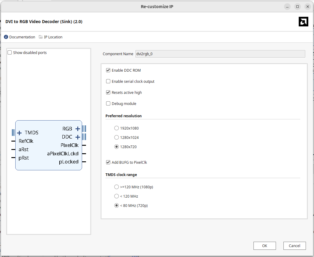
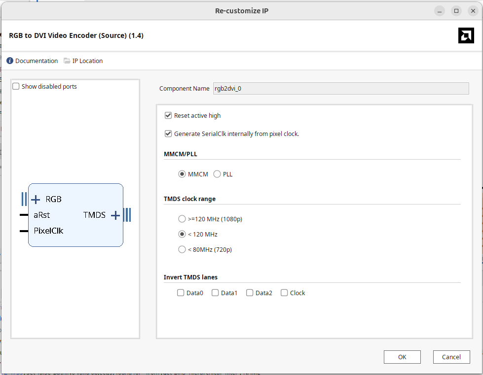
We're going to add two pieces of IP from the repository you just cloned: dvi2rgb and rgb2dvi. These two pieces are written in VHDL. The latter generates DVI/HDMI TMDS video signals just like you did in 6.205. The former, dvi2rgb does the opposite (which is arguably an easier task than what you already did in encoding it in 6.205).
The DVI2RGB module (data sheet here) is very helpful since it takes care of the DDC commands needed to convey to a video source the requirements (resolution, frame rate, etc...) of the sink. Normally a monitor does this, but our Pynq board is the monitor here.
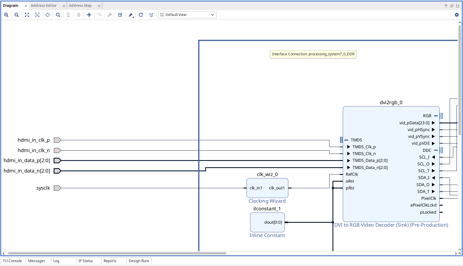
For the dvi2rgb, open it up, and configure it as shown below:
Add an RGB2DVI module as well and configure as shown below:
Clock Wizard
We need to make a 200 MHz clock to drive the DVI2RGB module. We could derive this from the FCLK0 from the Zynq PS portion, but that can be a little unstable and it would also be nice to have it always be on (and not need the PS itself to be up and "running"), so instead we'll bring in the external 125 MHz clock on the board that is routed to a PL-accessible pin (sysclk) and using a PLL make 200 MHz from it.
Add an Clock Wizard IP module and give it the settings shown in the figures below:
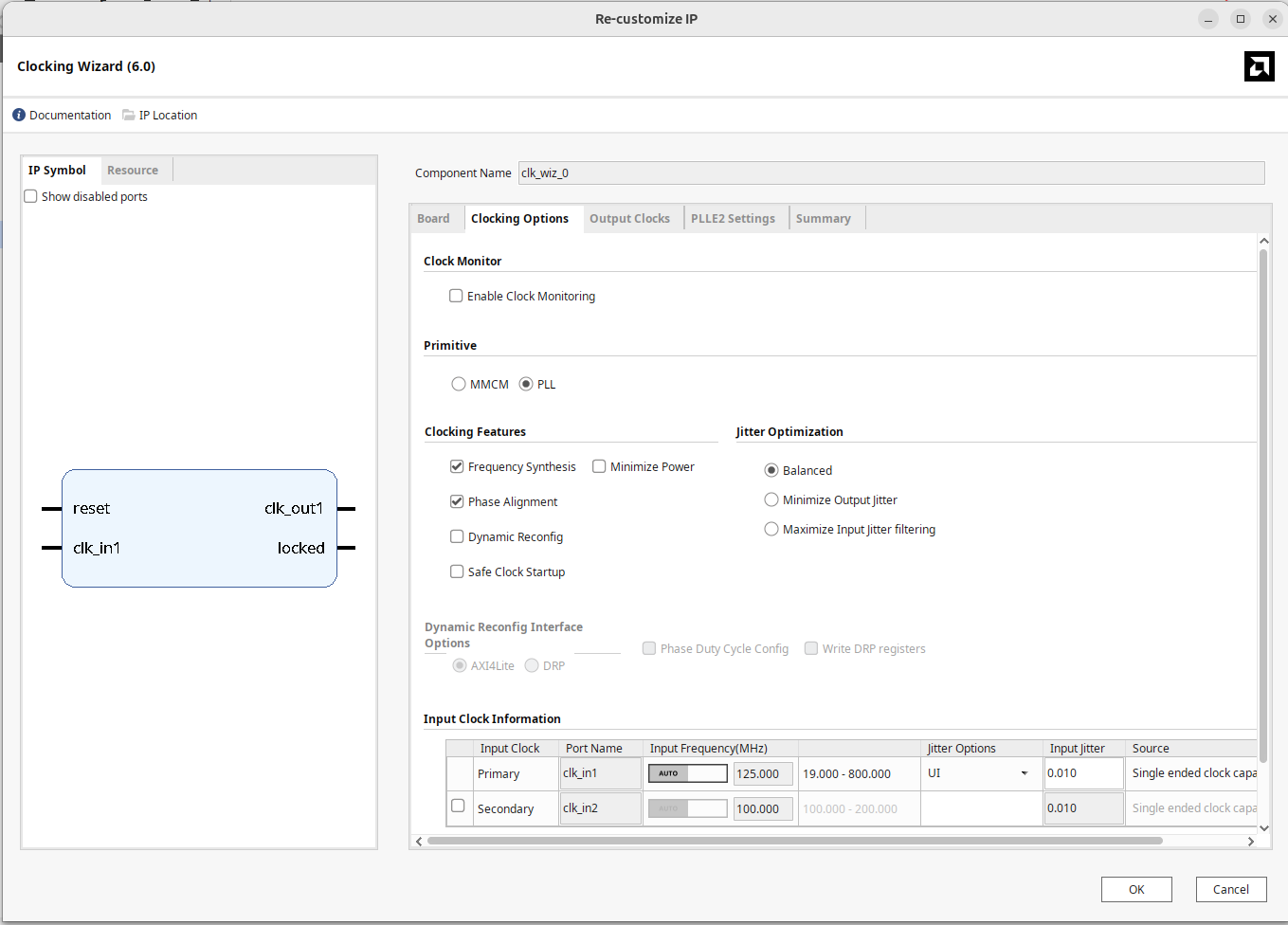
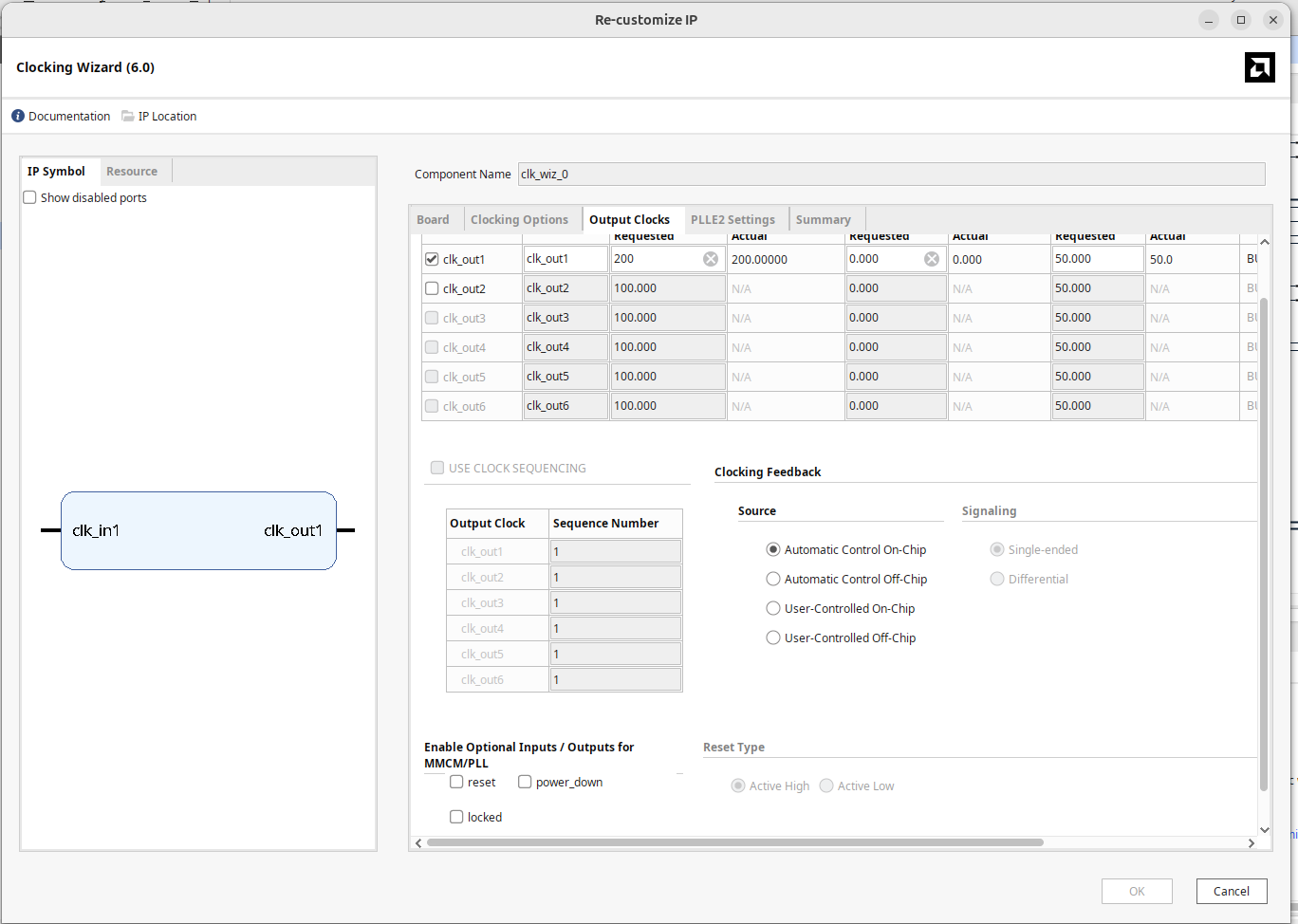
The output of the clock wizard should drive the RefClk Input of the DVI2RGB module
DDC Connections
Add in two instances of the tristate.v module that we gave you at the top of the page. Use one of them to interface the DDC connections on the dvi2rgb IP to the two inout ports you created. Tristate communication, where two parties convey information on one shared line, is tricky to get right and a common way to implement it is to have an input, and output, and then a control signal that you use to decide when you control the line or listen. The three components of a tristate channel, the I, O, and T signals achieve that.
For the SCL_I, SCL_O, and SCL_T signals, connect them to a tristate modules, O, I, and T ports, respetively and then connect the IO port of the tristate to the hdmi_in_ddc_scl_io port in the block diagram.
Similarly, for the SDA_I, SDA_O, and SDA_T signals, connect them to a tristate modules, O, I, and T ports, respetively and then connect the IO port of the tristate to the hdmi_in_ddc_sda_io port in the block diagram.
Some Constants
Some of the signals we have should be driven by Always-High or Always-Low constants. You can make that with "Inline Constant" IP.
The two HPD ("hot plug detect") pins need to be alway set to 1. The reset signals on our dvi2rgb and rgb2dvi modules need to be tied to 0 (and possibly others in the future. Add some to take care of that.
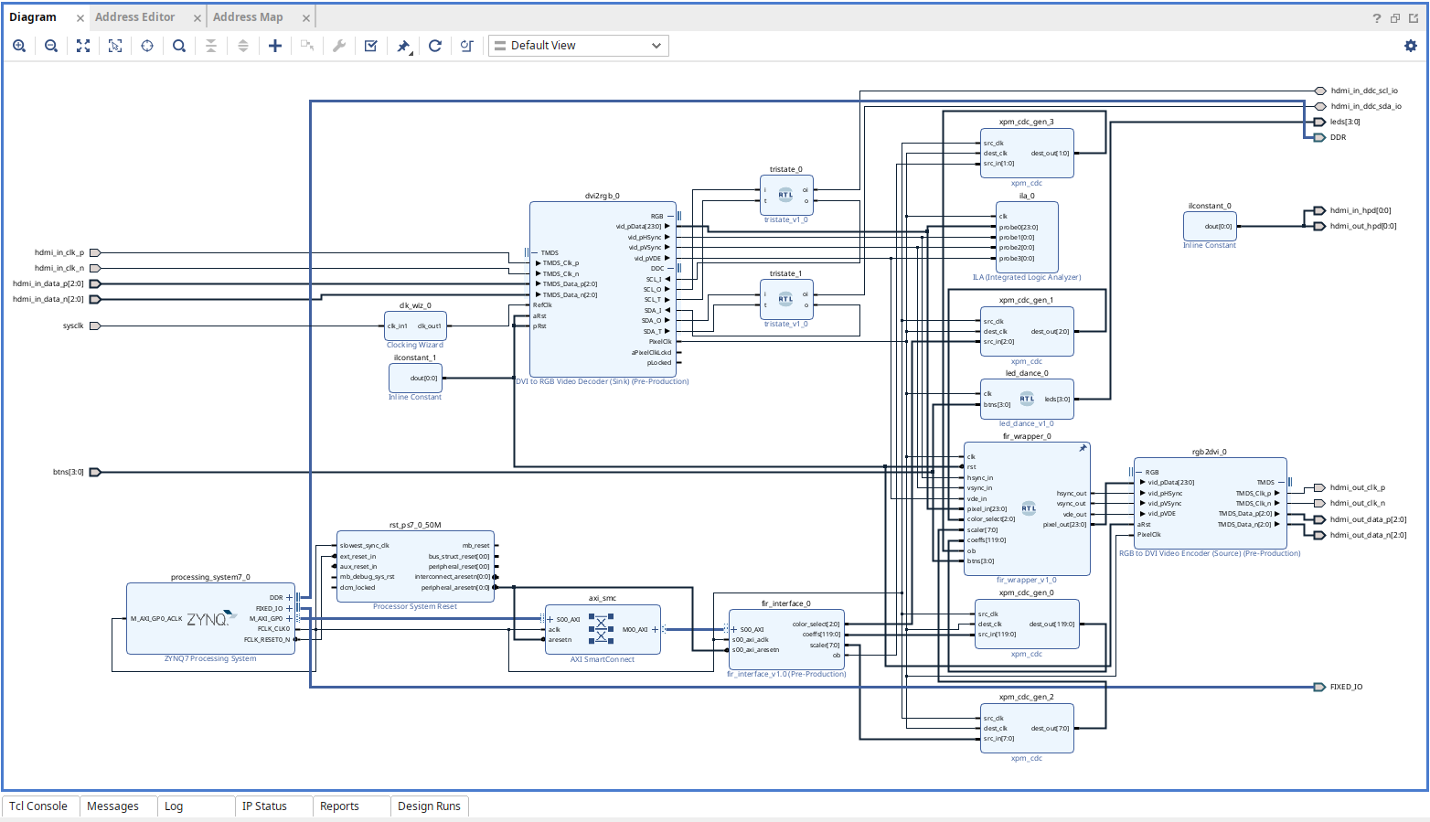
Check-In
As a bit of a check-in now, your connections for the modules we've talked about should be looking something like this:
OK hopefuly things are looking-okish...let's move on.
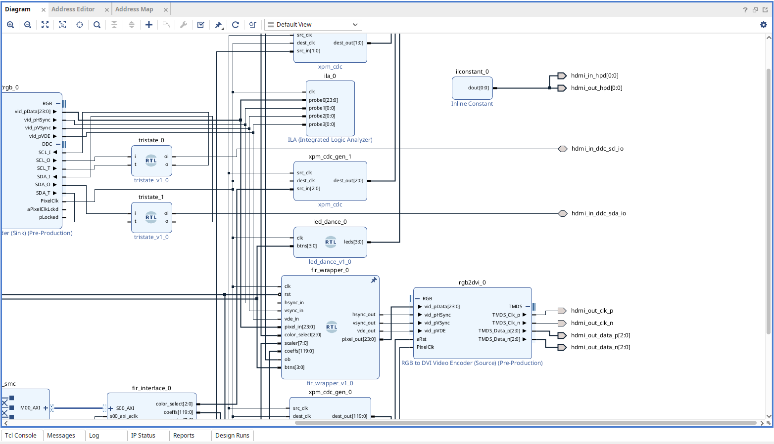
FIR Wrapper
Next we're going to connect the output of the DVI2RGB to the RGB2DVI, but in order to have cool stuff happen we should put our FIR filter that you built earlier into the pipeline. The fir_wrapper module provided at the top of the page (pure Verilog) is the thing for that.
This module is partially provided to you. What it does is take in the appropriate signals that will be handed to it from the FIR Interface MMIO and route them to the FIR modules (one for each color channel R, G, and B), as well has handle the channel splitting and recombining. That aspect should be already done for you so your FIR filter can live happily.
The entire system will be clocked off of the recovered pixel clock of our video stream (74.25 MHz). The hysnc, vsync, vde (active video), and pixel ports should connect to the appropriate outputs and inputs of the dvi2rgb and rgb2dvi modules. Also remember the clock. Also set the reset to always be 0 (note when creating the fir_wrapper, the reset signal may be shown as an active low in the block diagram. Vivado is supposed to be able to infer the correct polarity based on the signal name (rst), but it often doesn't...sigh quel dommage.
There are a set of control signals going into this module as well. The first four will come from an MMIO IP we'll specify below and one will just come from the board buttons.
color_select [2:0]: active high enable signals for the red, green, and blue FIR channels.scaler [7:0]: a term we'll use to shift back some of the gain our FIR filter builds up due to only using integers for coefficients.coeffs [119:0]: what is actually a[14:0][7:0]2-d array of coefficients for our FIR filter, but 2D-packed arrays in Verilog are annoying sometimes.ob: An offset binary value discussed below for shifting the signal space.btns[3:0]: Mostly used for debugging, but pressing them will turn off color channels (hook this up to the buttons).
Study the code of the fir_wrapper module. It is mostly working, but needs to carry out three additional support features that you'll often see used with FIRs (and other DSP pipelines):
- Offsetting (already done for you): The value that our pixels will come in at will range from 0 to 255 because it is 24-bit "true" color, with 8 bits for the red, green, and blue channels. In some applications, this range of numbers is fine. In others, it actually helps to shift this range of values to the range of -128 to +127. The
obsignal will control that. Whenobis set to 1, the system shifts the incoming 0 to 255 range to -128 to 127 range, runs it through the pipeline, and then unshifts it back to a resulting 0 to 255 range for output. - Scaling: (you need to do...should be one line): As you saw in testing your FIR, your output signal may be much larger than it was on the input because the coefficients are all whole numbers. This could be an issue. What needs to be done is after the FIR, the signal should be right shifted by the amount specified in
scalerinput. Remember about signs!!! - Clipping: (you need to do...needs a few lines): Even with shifting, values might end up outside our signal range so we need to make sure signals are clipped at their boundaries to avoid overflow or underflow artifacts (which will often appear as bright splotches of color where low values should have occurred or vice versa). These clipping boundaries will be based on whether or not
obis activated (ifob, the appropriate clipping range is -128 to 127, else it is 0 to 255).
Once you think you have it working, move on. (also note, just for reassurance) that this module should basically just be a pass-through of the video feed if you're worried you did the wrong changes up above.
FIR Interface
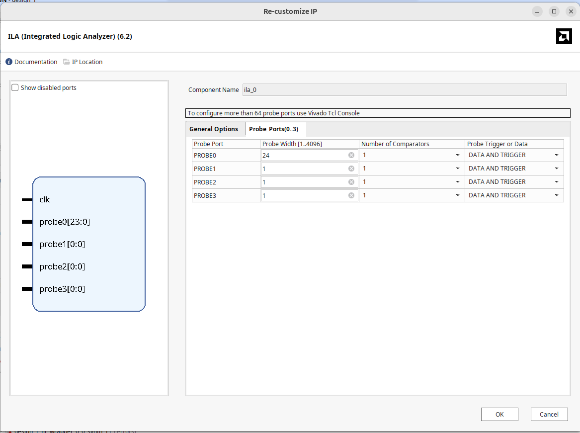
Next you need to make a piece of MMIO IP (just like last week). The module will allow us to transfer down (via Python) coefficients for our FIR filters that we just put in the video pipeline. Create the IP just like last week, but make sure it has 32 internal registers that you can write to instead of the 8 or whatever we did in week 2.
Have these values break out of this module (and then to eventually connect to the FIR filters).
output wire [14:0][7:0] coeffs,
output wire [2:0] color_select,
output wire [7:0] scaler,
output wire ob,
What are these four signals? Well they go with and control the FIR module we just talked about.
coeffsare your fifteen coefficients for your FIR that you've already designed. For simplicity, we just made our coefficients 8 bits, you'll remember, so that's why this array is a 15-long array of 8-bit values.color_selectspecifies which color channels (r,g,b) you want to apply filtering to.scaleris an 8 bit number that will be used to shift the result of our FIR downwards based on how much overall gain we anticipate.obis a simple command that is used to apply an offset to the color signal ranges, allowing us to view the pixels as either ranging from 0 to 255 or -128 to 127. While this isn't strictly needed, it can help us achieve different effects.
In building this module fir_interface, you're going to want
- Have all 15
coeffsvalues be set by slave registers 0 through 14. - Have
color_selectbe set by slave register 15. - Have
scalerbe set by slave register 16. - Have
obbe set by slave register 17.
We're going to make coeffs be a fully-packed array since Vivado works the best with that and can't support packed and unpacked dimensions in its ports for some reason. Note that even though we're making this a [14:0][7:0] array, it will appear as a [119:0] array in Vivado's block diagram. This is fine, just be aware! We talked about this in the FIR design on the previous page in this week's assignment.
Make sure the IP's AXI bus is using the AXI clock. Vivado's A.I. should be able to figure this out, but you never really know.
Clock Domain Crossing
Values you set on the MMIO interface will be on the AXI clock (whatever that might be). The FIR and its associated logic will be running on the 74.25 MHz pixel stream. These are two separate clocks. If you just hook the MMIO control values (coeffs, op, etc...) to the FIR wrapper, Vivado will take ten minutes to build, eight minutes of which will have been it trying in vain to meet timing when it never can, before giving up and saying timing is not met.
To fix this we need to add in some clock-domain crossing logic. We could do that with Verilog/SV, and specify it running through some synchronizer flops with a few directives to Vivado to know that the flops will fail timing, but we can also just use a default piece of IP for this. Search and add four instances of xpm_cdc IP for the four signals we need to transfer over. Make sure the widths for each module are appropriately sized for the four signals we're conveying. When wiring them up, make sure the src_clk is the AXI clock and the dest_clk is the PixelClk.
Add in a Logic Analyzer
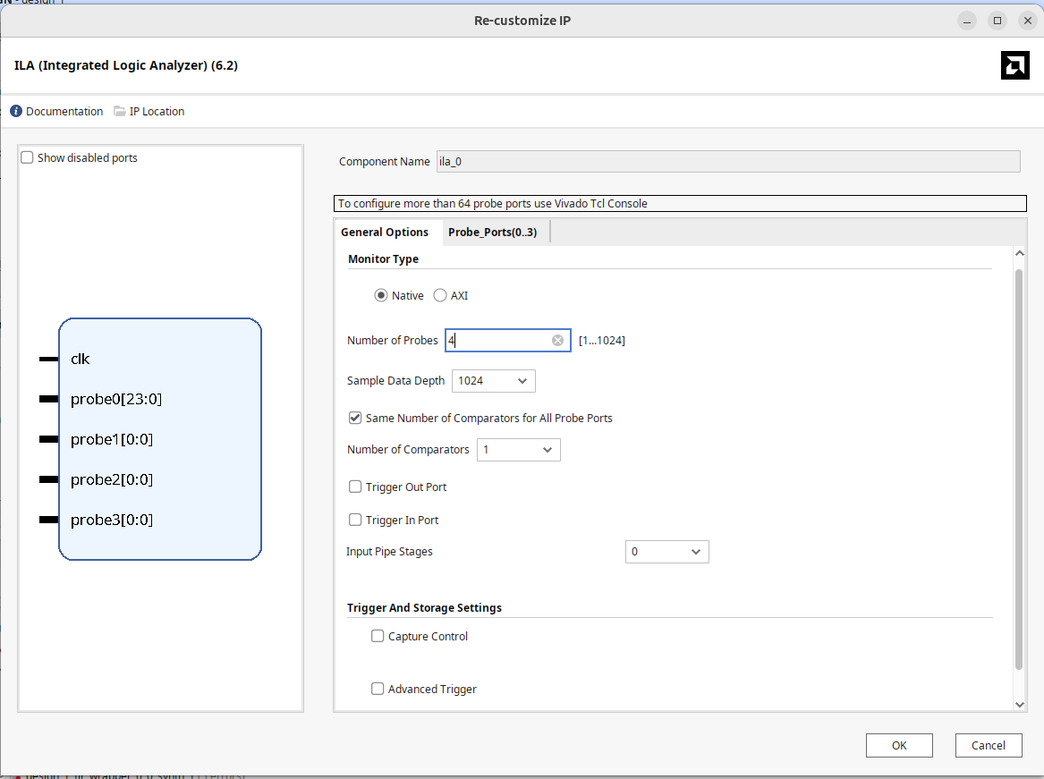
The (final?) piece of IP we're going to add in (because it is good to get practice with it), is the Integrated Logic Analyzer. This device actually let's you measure signals inside the FPGA while everything is running. It is a very powerful debugging tool.
Search for it and add while configuring it, add four ports with widths of 1,1,1, and 24 bits, which we'll use to read the hsync, vsync, vde, and pixel data on the video stream.
When hooking it up, connect it to somewhere in your video pipeline. I did it before the FIR-wrapper just to make sure the video was working in the first place.
Ok Maybe you're Good?
Your design should be looking roughly like this now. I have an "led dance" module I wrote for debugging earlier, and who knows, maybe you'll need to have something similar, but for the most part, you should be pretty close to this.
Generate Output Products, make the wrapper the top level, click all the buttons and hopefully get through a build. If that all passes, move on.
Into Snake Town (Python)
Move on over to the Pynq framework and let's see what is going on.
Make a new Python notebook and do a bare minimum set of lines that brings in the bit file and hardware handoff file you just made:
from pynq import PL
PL.reset() #important fixes caching issues which have popped up.
from pynq import Overlay  #import the overlay module
ol = Overlay('./design_1_wrapper.bit')  #locate/point to the bit file
Run it. If everything is hooked up we should have a functioning pass-through video device right now, requesting and conveying 720p video.
Hook up a HDMI cable to one of the HDMI out ports on a lab computer and then conenct it to the HDMI input of the the Zynq board. If everything is good on the input side, the computer should do that weird ice-cream-brain-freeze thing it does whenever you hook up a monitor and then come back to you. Take a second HDMI cable, hook it up to the HDMI output ort and then hook that up to one of the monitors at a lab station. Hopefully...within about ten seconds, you should be getting second-dispaly video on that monitor. If not...something is up and we'll need to debug.
Logic Analyzer Usage
Back in Vivado (yes Vivado) we now want to use the integrated logic analyzer either for debugging or just plain marveling at its operation. To do this we need the computer to connect to the FPGA over JTAG. This can be done by grabbing a USB cable and connecting from the computer to the PROG UART port on the board (we could have also used this for power all along actually, but we used an external supply instead).
In the lower left corner should be a "Open Hardware Manager" thing. Inside there. Click on "Open Target" and possibly "Auto Connect" if it prompts you. What should come up is what is effectively a logic analyzer dashboard. Pick the hw_ila_1 or (ila_0 if that's the one) device that is present. In the waveform window, add signals using the + button. Then run the arrow to just do a immediate (un-triggered) grab of data. The result (if you have video) should be something like below:
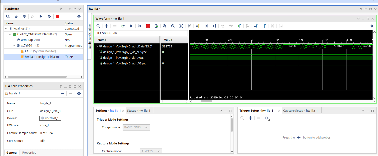
The ILA is very powerful. You can use it to monitor lots of actual signals (this is not a simulation...this is your actual, messed-up build). You can set quite complicated triggers with it. It is a great tool to have.
Controlling your FIRs
Ok we built an MMIO earlier. Now let's write some code to talk to it.
Assuming your FIR Interface was called fir_interface_0, the following code
import math
fi = ol.fir_interface_0  #find the AXI MMIO module which we can talk to (name of IP)
coeffs = [0,0,0,0,0,0,0,0,0,0,0,0,0,-4,4] #simple emboss kernel

#most kernels will have > unity gain. We need to undo this with a final shift.
#to calculate, sum the coefficients
#figure out the closest power 2 that sum is, then use to assign the shift amount
coeffs_sum = sum(coeffs)
shift_amt = 0
if coeffs_sum!=0:
    shift_amt = int(math.ceil(math.log(sum(coeffs),2)))
print(coeffs_sum, shift_amt)
#To set values in our MMIO:

#write coefficients (registers 0 through 15):
for i in range(15):
    fi.write(i*4,coeffs[i])
fi.write(15*4,7) #turn on all three channels (rgb) via reg 15
fi.write(16*4,shift_amt) #write shift amount to reg 16
fi.write(17*4,1) #turn on offset signal (signals processed as -128 to 127) (register 17)
d = fi.read(15*4) #read back for sanity
print(hex(d))
If you get something like this, then you are likely in a very good place. If not...you must debug....sorry.
Try a few additional kernels, including the ones you were testing and verifying your FIR with earlier. Experiment with the offset and or the shift (clipping may give good effects in the artistic sense, if not the signal-integrity sense).
During your checkoff you should be able to get signals similar to those shown below:
Show your working MMIO-controlled video streaming system to a staff member.

.v file (the product of all the block diagramming), as well as the completed fir_wrapper.v and your inner MMIO axi verilog file please! So three files in total!