RFSoC
The Next Board
Please Log In for full access to the web site.
Note that this link will take you to an external site (https://shimmer.mit.edu) to authenticate, and then you will be redirected back to this page.
The Setup
OK the goal today is to spin up the RFSoC. There are a few out at certain lab stations. No food at those lab stations. I'll fail you so hard if you're eating next to one of those RFSoCs. Most of what you're doing is going to be the same as if you were on the Pynq Z2 board so definitely make sure to refer back to those notes/pages.
Go in and make a new project just like before. Insteady of choosing the Pynq board, choose the RFSoC 4x2 board which you should have as an option on the lab machines. Click through everything else as before.
We don't need much of an XDC file for what we're doing but sometimes having some switches and LEDs is nice for sanity-check debugging. Use this below to make your XDC file:
## USER LEDS
set_property PACKAGE_PIN AR11 [ get_ports "led[0]" ]
set_property IOSTANDARD LVCMOS18 [ get_ports "led[0]" ]

set_property PACKAGE_PIN AW10 [ get_ports "led[1]" ]
set_property IOSTANDARD LVCMOS18 [ get_ports "led[1]" ]

set_property PACKAGE_PIN AT11 [ get_ports "led[2]" ]
set_property IOSTANDARD LVCMOS18 [ get_ports "led[2]" ]

set_property PACKAGE_PIN AU10 [ get_ports "led[3]" ]
set_property IOSTANDARD LVCMOS18 [ get_ports "led[3]" ]

## USER SLIDE SWITCH
set_property PACKAGE_PIN AN13 [ get_ports "sw[0]" ]
set_property IOSTANDARD LVCMOS18 [ get_ports "sw[0]" ]

set_property PACKAGE_PIN AU12 [ get_ports "sw[1]" ]
set_property IOSTANDARD LVCMOS18 [ get_ports "sw[1]" ]

set_property PACKAGE_PIN AW11 [ get_ports "sw[2]" ]
set_property IOSTANDARD LVCMOS18 [ get_ports "sw[2]" ]

set_property PACKAGE_PIN AV11 [ get_ports "sw[3]" ]
set_property IOSTANDARD LVCMOS18 [ get_ports "sw[3]" ]


set_property BITSTREAM.CONFIG.UNUSEDPIN PULLUP [current_design]
set_property BITSTREAM.CONFIG.OVERTEMPSHUTDOWN ENABLE [current_design]
set_property BITSTREAM.GENERAL.COMPRESS TRUE [current_design]
When ready, make a new block diagram design. Don't click automate/wiring until you've got all your pieces laid out.
We need to add some things:
The Processor
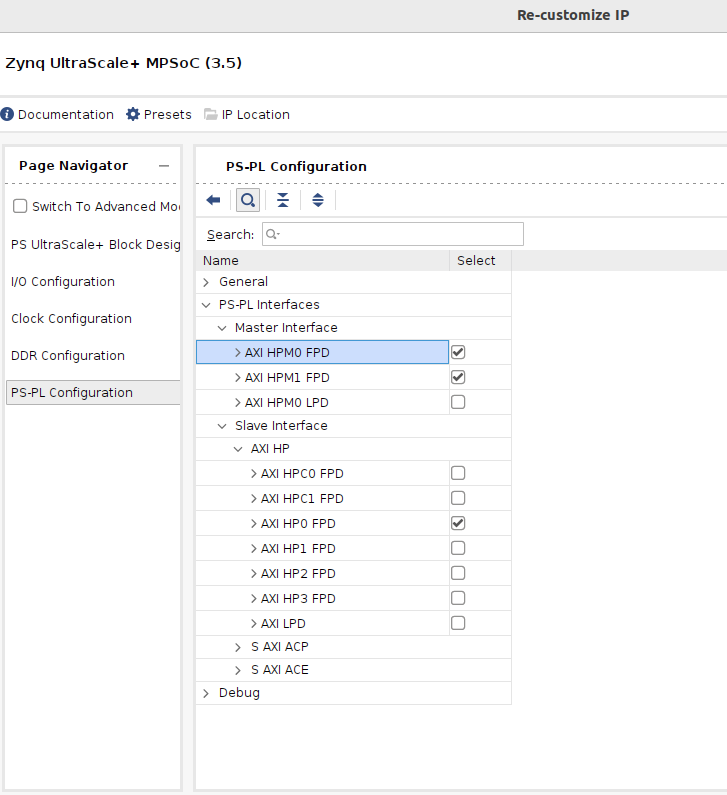
Make a processor like before. This will be fancier than the Zynq Series 7 one, but effectively the same thing, just with more options. We'll need
- two HP Master ports (one for the ADC and one for the DMA) and then...
- one HP Slave port (for the DMA).
I made them all 128 bits in size which is what they default to. These actually are the incorrect size for what is eventually needed, but using an AXI interconnect (which should get inferred) will resolve it. Details below:
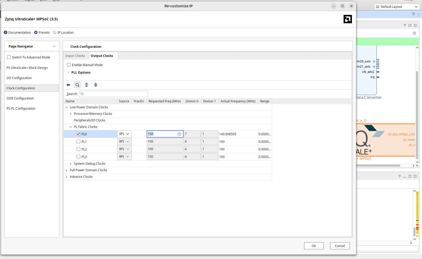
Also under the clocks/output-clocks tab, make sure you have peripheral clock specified like shown below. Set the clock to 150 MHz (important!):
Don't Even THINK about making Vivado auto-connect stuff yet. It has no idea what to do so hold off.
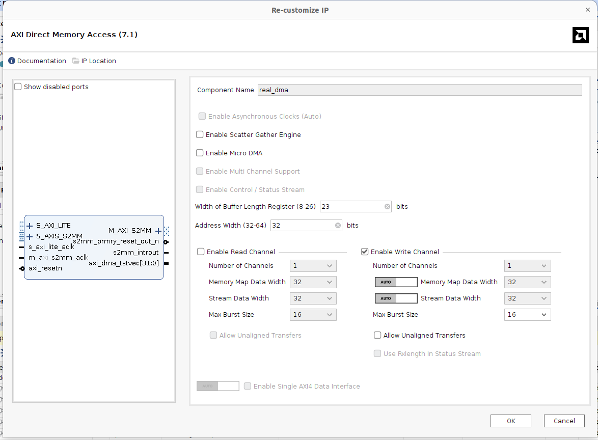
The DMA module
The DMA can be very simple (just like before). This will require one fresh DMA. We're not going to be reading from the DMA (from the perspective of the PL, mind you), only writing...so we only need a write channel (just like in week 5). Settings I used below are shown. Make sure scatter-gather is disabled, though that probably doesn't matter (but I haven't tested it).
RF Data Converter
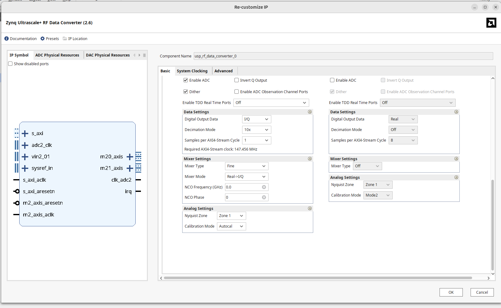
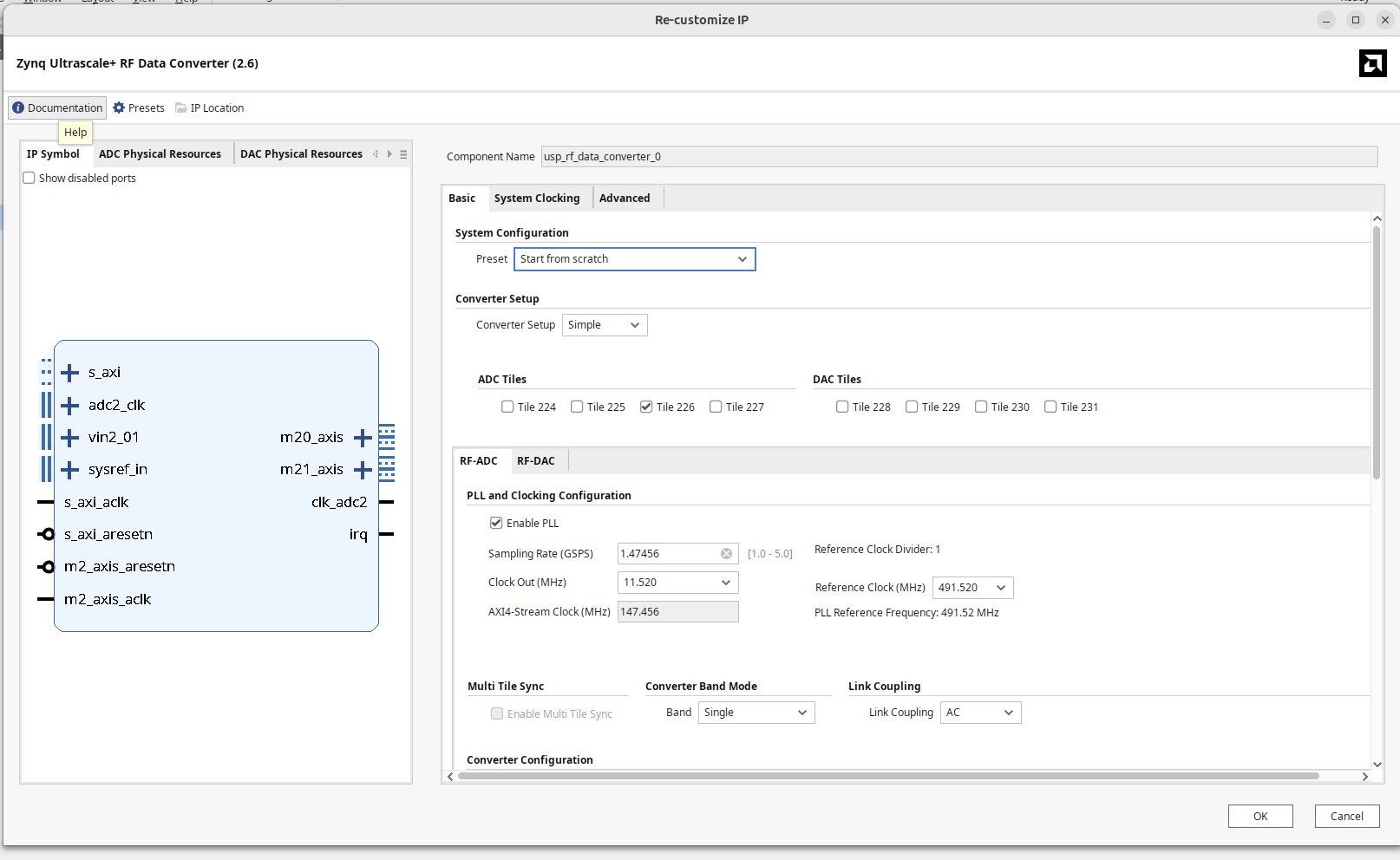
OK now we need to add "the new thing". The RF Data Converter. Search for the Zynq RF Data Converter IP and add one to the block diagram. The Data converter is running off of the external 491.52 MHz1 crystal oscillator. There's no way for Vivado to know what the RFSoC is actually connected to so we need to tell Vivado that information. Vivado does not want to be told that so we need to trick it into understanding it, just like you trick a child into eating their vegetables by going "mmmm this tastes so good. nom nom nom" or something....there's a whole process...so:
Open it up to customize the IP:
- First, specify the Converter setup as "Simple"...lol.
- Then activate ADC Tile 226.
- Then scroll down and under Converter Configuration check "Enable ADC" under ADC 0.
- Set the Digital Settings to:
- Output Data to "I/Q"
- Decimation Mode to "10X"
- Samples per AXI4-Stream Cycle to "1"
- Under Mixer Settings:
- Mixer Type to "Fine"
- Mixer Mode to "Real->I/Q"
- Analog Settings:
- Nyquist Zone: "Zone 1"
- Calibration Mode: "Autocal"
- Now we can't tell Vivado the crystal frequency is 491.52 MHz directly, instead we have to let it figure it out. Scroll back up and under PLL and Clocking Configuration, check the "Enable PLL" box, and then set the sampling rate (GSPS) to 1.47456 ( multiple of 491.52 MHz). Now scroll over and you should see a bunch of options that Vivado figured out for you about what the Reference clock is. Find 491.520 and pick it. Do you see two of them? That's fine just pick one of them. Why are there two of them? I mean come on...this is Vivado, the more appropriate question is to ask why there aren't two of all the other frequencies. Just be happy the GUI pulldown is mostly working.
- Ok next, make sure "Clock Out" was correctly inferred to be 11.520. and that AXI4-Stream Clock is 147.456 MHz. If they aren't you probably messed up one of your earlier settings somewhere.
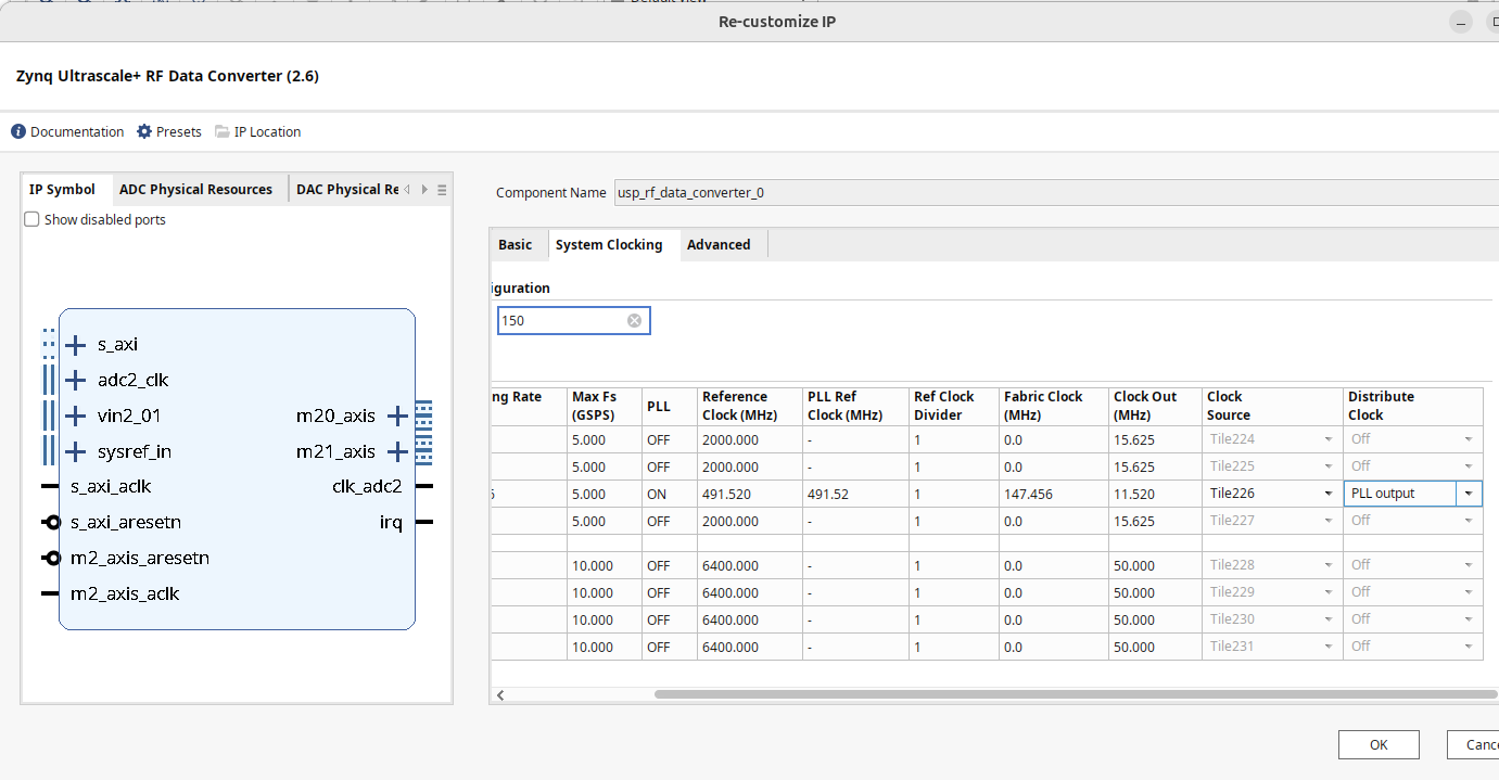
- Now on the "System Clocking" tab, first set the AXI4-Lite Clock to 150 MHz (to match the value we set earlier) and then verify all the numbers for ADC 226 are correct (1.47456 Gsps sampling rate, PLL Ref Clk of 491.52 MHz, Fabric Clock of 147.456 MHz, Clock Out of 11.520 MHz, and set Distribute Clock to "PLL Output"
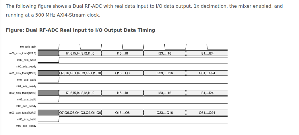
Ok some images of this journey (in no particular order) are below for reference:
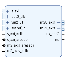
Anyways this newly configured piece of RF grabbing IP should look like this:
A Clock
We now need to make a fabric clock that identically matches the output sample rate of our ADC which is 147.456 MHz. To do that we'll use the 11.520 MHz output clock from the ADC and a clock wizard to generate that. Add a clock wizard, deactivate the reset and lock signals, and set it up with the appropriate input and output values:
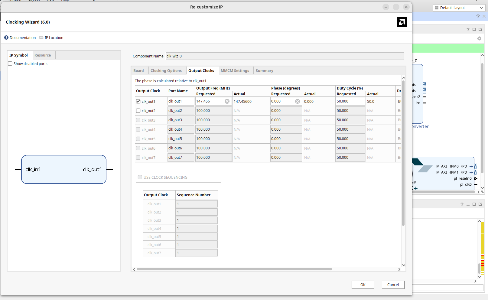
Hook that thing's input up to the output of the RF Data Converter (its clk_adc2 signal)
A Piece of IP You Must Make
OK, the RF Data converter will work as it is, but without any context/packaging, it is tough to get it into the PS side. As a result, there's a few things we want to do to "package" the data stream coming out of it. We'll wrap all of that functionality up into a single piece of IP which I'll call "iq_framer", but you can call it whatever you want. This piece of IP will live between the RF data converter and the DMA. All of its ports are shown fully-expanded out:
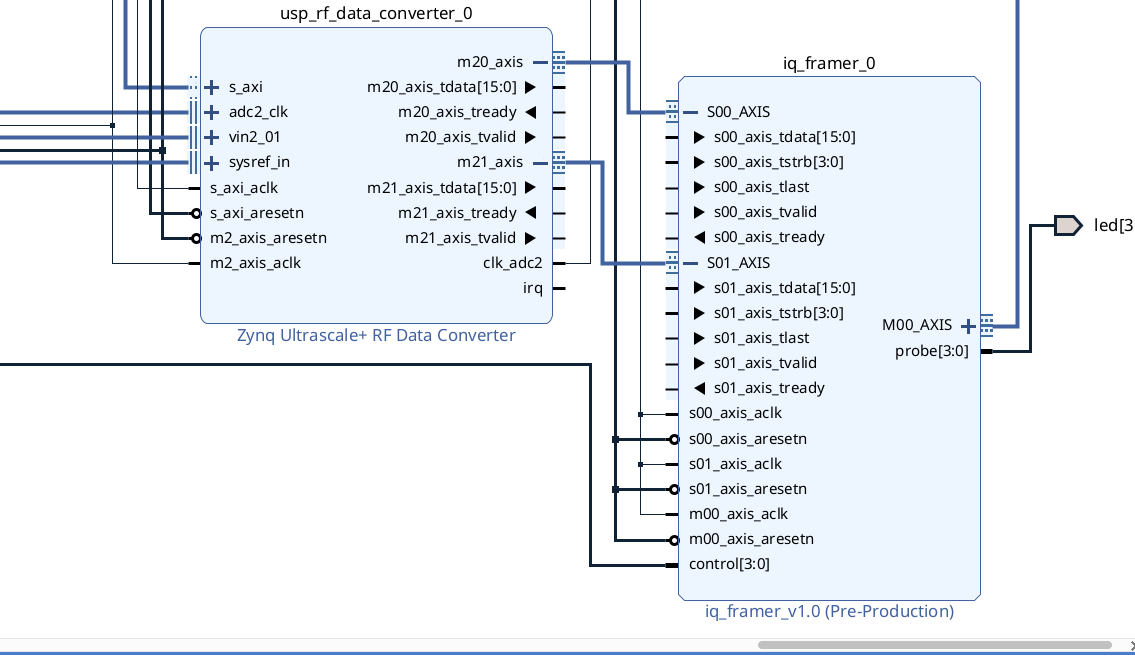
This thing has to do several primary tasks:
Task 1: Merge Channels
The output of the DDC as configured will produce two independent AXI Streams containing the I and Q data from the complex down-mixing. This is a weird choice in my opinion since an I/Q pair of values really should move through life together...and adding to the mystery, each I/Q value is signed 14 bits so you could easily fit both in a stacked format within a standard 32 bit AXI Streaming data channel , but who am I (or Q...heheh you get it?) to question. Instead, of course, the I and Q values come out in two non-standard 16-bit AXIS busses, complete with their own READY and VALID signals, etc... The READY signal doesn't do anything and the RF Data converter ignores it regardless of the design configuration in my experience. The VALID signal, in this configuration will always be high.
To get them into the DMA we need to merge them together into one channel, (or alternatively we could have two DMA blocks with each written to that...but the DMA needs to be 32 bits I believe...so then you'd be running at 50% bandwidth efficiency...)...so we'll just instead merge our two streams into one 32 bit stream.
The data sheet (taken from here) implies that both channels are perfectly synchronized and in my testing this seems to be the case (which further adds to the mystery of why not putting them in one stream in the first place, but whatever).
So we need to make this piece of custom AXI streaming IP take two AXI slave ports and merge them together with this in mind. The fact that they are perfectly synchronized means you can just use both valid signals together to decide when to sample both and then just feed the TREADY back pressure signal back through one module and call it a day. In a real AXIS-merging device you'd have to do some fancy cross-checking logic to deal with the unsynchronized issues of the two input streams, but that doesn't seem to be needed here.
So I took my two measurements I/Q values and stacked them...I on the lower 16 and Q on the top 16. This should be good enough for this lab.
Task 2: TLAST
The second big issue is that the data which comes out of our RF data converter will just be sample after sample with no context or framing to them. Unfortunately, we can't just feed this data stream into a DMA Slave AXIS port because there's no TLAST signal on it...which means when you try to read/wait for the DMA write transation to take place, you'll hang forever (think back to the FIR stuff you worked on and the bugs with that)...this was also what you did in week 5 with the data framer module. We need to add a TLAST signal to it. This is going to be basically the simplest framing we can. For this I used an internal counter capable of counting up to 262143 (2^18-1). Based on the input values of the control signal (which I tied to my switches), a TLAST signal would fire either every 65536 samples or 262144 samples. As a result, we just repeatedly and periodically send in transfers of data that are "framed" with the TLAST signal.
In practice the DMA is not always ready to read, so it will normally, when we're not prompting it in python, hold up the show, and that's fine with this...the ADC samples will just get lost, but we have nowhere to put them anyways except for a little bit of a FIFO that we'll add for clock-domain crossing in the next part. But when we do go in and do a READ as long as we tell the DMA transfer to be a size larger than 262144 measurements (4 bytes per measurement), because what we're writing to memory via the DMA will be smaller than that python won't hang...it'll be guaranteed to get a TLAST signal in within that wait period. Adding debug signals here isn't a bad idea either. I did something like:
	assign m00_axis_tdata = control==1?{valid_counter, valid_counter}:
	                        control==3?{s_counter, s_counter}:
	                        {s01_axis_tdata, s00_axis_tdata};
which then allowed me to set sanity check values like a ramp which could be plotted in the notebook using some of the switch values (i used other switch values to specify the burst sizes)
So build that piece of IP (it should be pretty simple and I'd honestly just suggest writing it in regular Verilog in the top-level of the IP you create (delete those default Master/Slave Stream bus managers it puts in there).
Hints:
When making the IP, make sure to have two Streaming S ports and one Streaming M port.
I directly edited the top file they give you after deleting all their boilerplate AXIS-manager modules. They're not needed here.
The output of the RF Data Converter is a pair of 16-bit AXIS data channels. Unfortunately Xilinx won't allow you to make 16 bit AXIS data channels (32 is the minimum) so this causes a mismatch. In the boilerplate code that you're given you can try to change parameter integer C_S00_AXIS_TDATA_WIDTH and its friend parameter integer C_S01_AXIS_TDATA_WIDTH to be 16, but when you package the IP it won't build since it'll see those parameters and say that's not allowed. This is quite hypocritical right? Similar to when your parents tell you not to smoke cigarettes and then they tell you about how they used to smoke cigarettes. What's the solution? Well you pay an older teenager to go and buy you a pack of smokes...which in this analogy means you keep those parameters at 32 so Vivado is happy, and then just manually make the data ports on s00 and s01 be half the width of C_S00_AXIS_TDATA_WIDTH like I do here. Yep this will work and let you build 16-bit wide AXIS data busses🙃. Nice try, Vivado.
As as I said, I added a 4-bit input (control) for debugging and TLAST/burst setting as well as a 4-bit output (That I connected to LEDs during my debugging) as well. Never a bad idea to add in some sanity checks to make sure your stuff is even just kinda working.
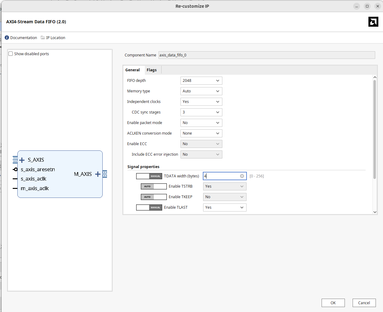
FIFO
OK the data rate of our ADC is 147.456 MHz, but the DMA will be running at 150 MHz (the clock we set six hours ago at the top of this lab writeup). This is a mismatch and to resolve this, we'll use a AXIS4 Streaming FIFO. Make sure this is a dual clock thing...also make sure to enable TLAST propagation!!!!
Resets
Ok we're going to have two different AXI clock domains going on now. To help the Vivado auto-wiring thingy work out, we need to guide it a bit more. Add in two processor System Reset IPs. For both of them, connect their ext_reset_in signal to the the pl_resetn0 signal from the Zynq PS block (this let's us reset the system from the Python). Then use the pl_clk0 (which should be set to 150 MHz) from the Zynq PS block to slowest_sync_clk on one of them and use the output of your clock wizard (making 147.456 MHz) to drive the slowest_sync_clk on the other one.
Both of these modules do the clock-domain crossing and give us reset signals for both clock domains.
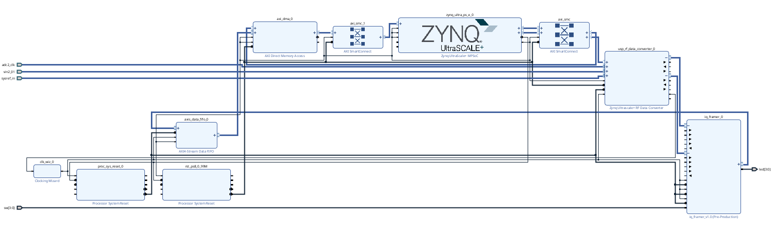
Wire it All Up
Ok a lot of crap on this block diagram now. We need to connect it together. We'll do some if it and then have Vivado finish the rest.
- Attach the output of the clock wizard (147.456 MHz) to:
- The
m2_axis_aclkon the RF Data Converter. - All the clocks on your
iq_framermodule. - The
s_axis_aclkon the AXIS FIFO.
- The
- Attach the 150 MHz clock from the PS (
pl_clk0) to:- All the clocks on the DMA (should be two of them)
- the
m_axis_aclkon the FIFO (output clock) - The
s_axi_aclkon the RF Data converter (this AXI bus controls the configuration of the ADCs) - All the various clock inputs on the Zynq module.
Using the clock domains specified above as a guide, then route the reset signal for each clock domain to the appropriate module ports, paying attention to names.
Finally, do a couple AXI connections.
- Route the two AXIS outputs of the RF Data converter to the two inputs of your IQ framer
- Route the output of your IQ framer to the input of the FIFO
- Route the output of the FIFO to the Streaming input (
S_AXIS_S2MM) of your DMA.
Also if you're using the switches and LEDs for debugging/control, route them to your IQ framer module.
Now this should (big emphasis on should) be enough for Vivado's A.I. to auto connect and route the rest. Up in the right is the "automate routing" prompt that is coming up. Click on that....and then likely click again...and possibly a third time. One thing to keep an eye out is if Vivado automatically reactivates the GPIO on the Zynq processor...if it does, go into the IO options and turn that stuff back off. Also Vivado may try to put your FPGA fabric clock (from the processor) back down to 100 MHz. Double check that since that can cause sampling issues eventually. I don't know what it is with 2025 wanting to do these things.
My layout looks like the following:
When ready, go ahead and build and everything like before. The generation of output products, in particular for the RF Data Converter takes a decently long time so be prepared.
Also you need to add a license to your Vivado in order to build. Here are the license files for machines 33 to 48 (inclusive) in the lab:
- machine 33
- machine 34
- machine 35
- machine 36
- machine 36.5
- machine 37
- machine 38
- machine 39
- machine 40
- machine 41
- machine 42
- machine 43
- machine 44
- machine 45
- machine 46
- machine 47
- machine 48
Put on the Board
OK Now it has to go onto the RFSoC. You need a fresh/new SD card for this. I have them at the front in special little holders for you.
Put one into an available, RFSoC, power it on, let it boot up (it'll take a minute or two) and when it is completed, the OLED in the middle will display the IP Address of the board (omg).
You should be able to just go to that IP address and find the device on the network just like before.
Upload the hardware handoff file and the bit file like before.
Then let's make a new notebook.
First let's do the old regular stuff (load the bit file/overlay, etc.)
from pynq import PL
PL.reset() #important fixes caching issues which have popped up.
import xrfdc #poorly documented library that handles interfacing to the RF data converter
from pynq import Overlay  #import the overlay module
ol = Overlay('./design_1_wrapper.bit')  #locate/point to the bit file
import pprint
pprint.pprint(ol.ip_dict)
dma = ol.axi_dma_0 #might need to change name depending on what you called it
rf = ol.usp_rf_data_converter_0 #might need to change name depending on what you called it
from pynq import Clocks
Clocks.pl_clk0_mhz = 150
print(Clocks.pl_clk0_mhz)
The last two lines grab handles to constructs we've created. The DMA you know and love already. The RF one is a handle to our RF converter. We can study and manipulate its settings as needed.
The ADC we activated is on the third ADC tile ("226" or index 2) and is the first tile (index 0). We need to grab a software handle to it and check its status.
adc_tile = rf.adc_tiles[2]
print(adc_tile)
adc_block = adc_tile.blocks[0]
print(adc_block)
print(adc_block.BlockStatus)
print(adc_block.MixerSettings)
adc_block.Dither = 0 #doesn't really matter for this lab, but let's turn off.
center_frequency = 1 #nothing there. but not zero to help with IQ issue
adc_block.MixerSettings['Freq']= center_frequency # set the frequency of the Numerically controlled oscillator.
adc_block.UpdateEvent(xrfdc.EVENT_MIXER) #every time setting is changed, must call this.
print(adc_block.MixerSettings)
And finally some stuff that grabs data, chops it up into I and Q and then plots it the spectrum!
import numpy as np
import time
%matplotlib notebook
import matplotlib.pyplot as plt
from pynq import allocate
def plot_to_notebook(time_sec,in_signal,n_samples,):
plt.figure()
plt.subplot(1, 1, 1)
plt.xlabel('Time (usec)')
plt.grid()
plt.plot(time_sec[:n_samples]*1e6,in_signal[:n_samples],'y-o',label='Input signal')
#plt.plot(time_sec[:n_samples]*1e6,in_signal[:n_samples],'y-o',label='Input signal')
plt.legend()
def iq_plot(time_sec,re_signal,im_signal,n_samples,):
plt.figure()
plt.subplot(1, 1, 1)
plt.xlabel('Time (usec)')
plt.grid()
plt.plot(time_sec[:n_samples],re_signal[:n_samples],'y-o',label='I signal')
plt.plot(time_sec[:n_samples],im_signal[:n_samples],'g-o',label='Q signal')
#plt.plot(time_sec[:n_samples]*1e6,in_signal[:n_samples],'y-o',label='Input signal')
plt.legend()
def plot_fft(samples,in_signal,n_samples,):
plt.figure()
plt.subplot(1, 1, 1)
plt.xlabel('Frequency')
plt.grid()
plt.plot(samples[:n_samples],in_signal[:n_samples],'y-',label='Signal')
#plt.plot(time_sec[:n_samples]*1e6,in_signal[:n_samples],'y-',label='Signal')
plt.legend()
# Sampling frequency
fs = 147.456
# Number of samples
n = 65536
T = n/fs
down_from_center = center_frequency - fs/2
up_from_center = center_frequency + fs/2
# Time vector in seconds
t = np.linspace(0, T, n, endpoint=False)
# Allocate buffers for the input and output signals
ns = np.linspace(down_from_center, up_from_center,n,endpoint=False)
out_buffer = allocate(400024, dtype=np.int32)
# Trigger the DMA transfer and wait for the result
start_time = time.time()
dma.recvchannel.transfer(out_buffer)
dma.recvchannel.wait()
stop_time = time.time()
hw_exec_time = stop_time-start_time
print('Hardware execution time: ',hw_exec_time)
real = []
imag = []
#extract the two values (I and Q) from each 32 bit write from the hardware side.
for i in range(65536):
val = out_buffer[i]&0xFFFF
if val>=32768:
real.append(np.int32(0xFFFF0000|val))
else:
real.append(val)
imag.append((out_buffer[i]>>16))
# plot_to_notebook(t,real,6500)
# plot_to_notebook(t,imag,6500)
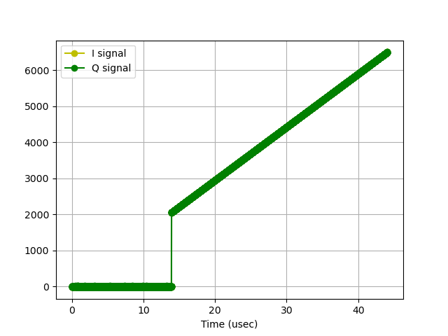
iq_plot(t,real,imag,6500)
#i flipped my real/imag I think and was lazy so fixed here
c_data = 1j*np.array(real) + np.array(imag)
z = np.fft.fftshift(np.fft.fft(c_data,n))
plot_fft(ns,abs(z),65535)
out_buffer.close()
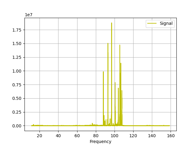
Now if you go and run this code you'll get a time plot of this (or something similar):

And a frequency plot of this:
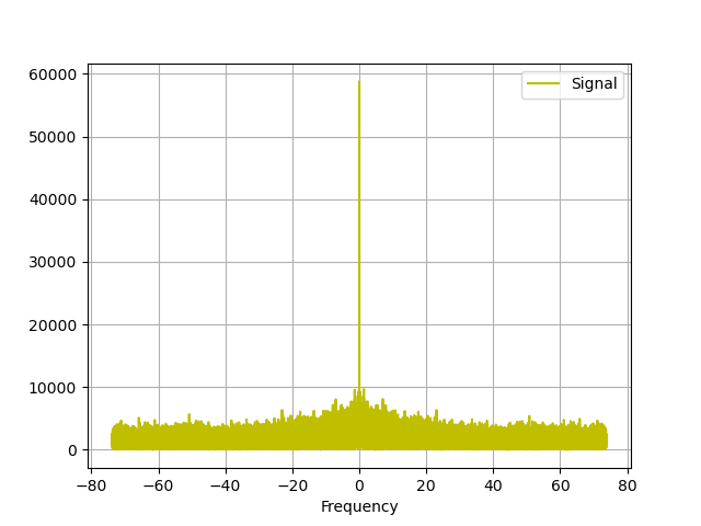
OK you've measured basically nothing and seen nothing. While not exactly a result that will win a Nobel Prize, it at least should hopefully check out. Is there anything out there that we could measure? If you added debug signals to your IQ framer, you can turn them on and see. I had the counter just get put on I and Q and got a time plot like this which is good (note depending on the FIFO size, there will be a build-up of the previous collection too...hence the silence followed by the jump to a ramp).
Now that we know stuff is hopefully coming through, is there anything legitimate we could measure? Why yes, let's jam an antenna on and see if we can capture a signal out of the ether. Around lab there should be some FM antennas that look like this:
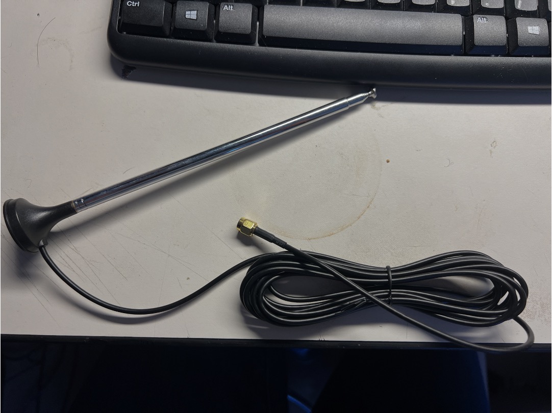
Grab one and attach it to ADC_B on the RFSoC. Commercial FM lives in the 88 MHz to 108 MHz frequency band. Our current effective ADC output sample rate is 147.456 Msps. This means there's no hope of getting that signal within our sample rate (though we will likely see it showing up in aliased images). But we do have a complex mixer at our disposal. We can set that things frequency to be a value that will then mix with our incoming signals to move that band down. (based on the f_s\pm f_m math we've talked about in class).
For a mixer frequency we'd want to pick something in the FM band on near there. 85 MHz might be a good choice. Since it would move the entire FM band down to base band and could easily fit within 100 MSps bandwidth. To do this you could try this in the second block...
center_frequency = 85
Then run (perhaps several times to flush the FIFO) the second block and suddenly...there is signal where there was none. We've pulled FM down into our baseband window.
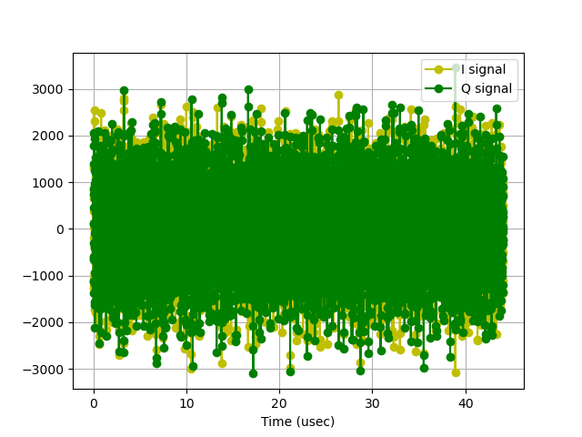
The time domain is gonna look like a mess since there' just signals on top of signals....but the frequency plot looks even cooler...
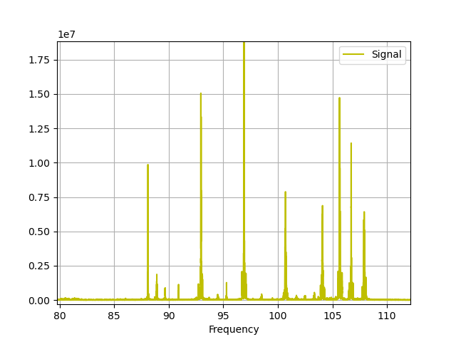
Your plot should look pretty close to this...if not, you maybe have some clocking issues (which can show up as frequency artifacts and things).
Frequency is across the X axis here.
Zooming in on one of the large spikes you can actually see a complete FM commercial station in the frequency space. The big spikes going left to right are:
- 88.1 MHz WMBR (MIT's college radio station)
- Bloomberg 92.9 WBOS
- HOT 96.9, which is #1 for Throwbacks and Today's Best Hip Hop
- 100.7 WZLX: Boston's Classic Rock
- 104.1 WWBX: Mix of music
- 106.7 WMJX: relaxing music
- Kiss 108 WXKS-FM which isn't nor does it claim to be transmitting hot information, but does assert it is the #1 Hit Music Station in Boston. Right at the boundary of the commercial Fm Spectrum.
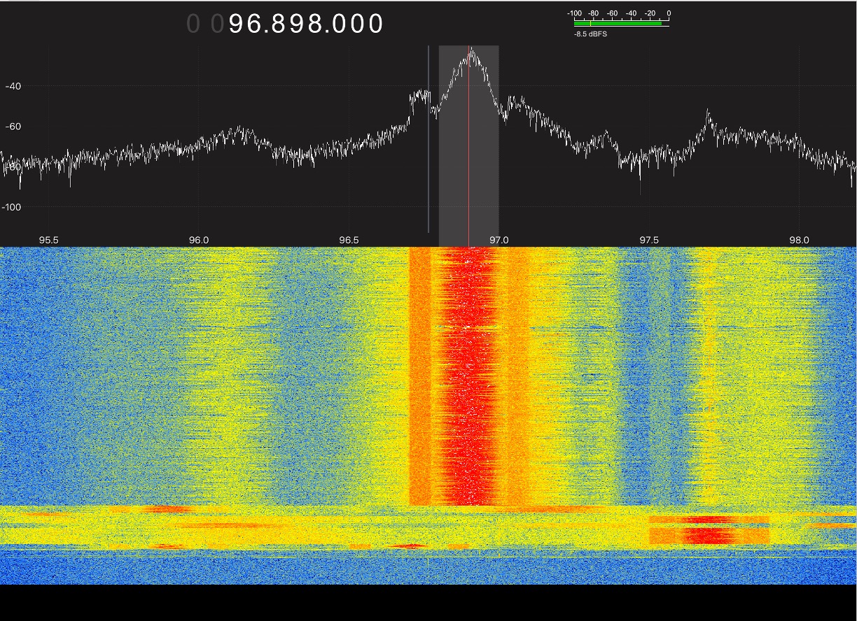
Since not everyone in the year 2025 knows what an FM station looks like in frequency space, here is a screengrab of one off of one of my Software Defined Radios.
The fact that we can see this signal raw with no amplification is a testament to the strength of commercial FM stations (there are transmitters literally across the river on the top of the Prudential Building).
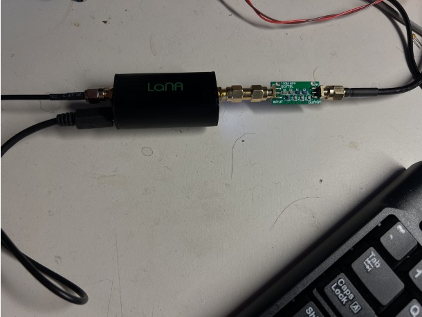
If we wanted to improve our signal-to-noise we should amplify and target our signal more. To do this, I have a couple Low-Noise-Amplifiers and a few FM-band-pass filters in lab. Connect the antenna to the input of the LNA, the output of the LNA to the input of the filter, and then the output of the filter to ADC_B. Make sure the LNA is powered...
I only have a few of these filters
Re run and you should have much larger signals that are much, much further above the noise.
Play around, look at signals. When you are satisfied, ask for the checkoff.
Show your working RFSoC system

Footnotes
1 Also why is the crystal oscillator 491.52 MHz? That seems like a weird number. It is a clean multiple of many other widely used frequencies, including the classic 24.576 MHz. Why is 24.576 MHz used? Because it was used in a lot of digital video technologies (and can be divided cleanly by 512 to get 48 kHz which is a common sampling frequency from the 80's). Why was 48 kHz used? Because that was sufficiently above 40 kHz which is 2X the upper limit of human hearing (generally accepted as 20 kHz). Why 48 though? I think because previously some standards used 32 kHz and 48 kHz was a nice 1.5X ratio increase. Why 32 kHz? Because FM standard broadcasts only did 15 kHz of audio...so 32 was again roughly 2X and then some above the highest frequency. Why was 15 kHz used for FM? Because that was the compromise number that was clean enough to allow through high fidelity audio but then kept the bandwidth of the overall signal narrow enough to use multiple Bessel function peaks (the larger your signal bandwidth, the larger those peaks would have existed out and the larger your overall bandwidth). Why is 15 kHz bandwidth good enough for FM? Since almost no instrument uses frequencies up that high. Why are no instruments utilizing that frequency space? Humans can barely hear up there anyways. Why is that? There was no evolutionary advantage to listening that high...we don't eat bugs and other things very much so what's the point.