Pynq 02
Doing more...
Please Log In for full access to the web site.
Note that this link will take you to an external site (https://shimmer.mit.edu) to authenticate, and then you will be redirected back to this page.
A Simple Memory-Mapped Interface
In this lab we'll look at making a Memory-Mapped piece of IP on the PL and then access it from Python (the PS). This will be used to control the MAX7219 display. The performance won't be amazing, but also this display doesn't actually need great performance, with its 256 one-bit pixels so this is relatively forgiving. It also has a very simple communication protocol so we hopefully won't get caught up seeing the forest for the trees (or whatever the saying is), instead letting us explore the overall pipeline of a Memory-Mapped Interface allowing a convenient and scalable interface between the PL and the PS.
Getting Started
So, I'm assuming you already did the first lab with Pynq. We can skip a lot of "click here" steps, but of course refer back to that as needed.
Start by making a new project targeted for your PYNQ-Z2 board. Add the same constraint file as last week. When setting it up, make sure that you specify the Board File rather than just choose the correct chip.
Once you're in your new project, go to your xdc and comment out everything except the four leds, the four buttons, and three of the "Arduino GPIO" pins. We just need three and any three should work, but I used the three corresponding to BGA pins T14, U12, and U13. I named them cs, data, and dclk, respectively.
create a new block diagram like before, and add a ZYNQ Processing System. Run the connection automation right away.
Remember to allow it to run the self-automation on the Zynq core!! This configures the clock frequency among other important things.
Add four output ports to correspond to the four things left in your xdc file:
csdatadclk[3:0] leds[3:0] btns
Note in making these ports, feel free to leave them all as type "other" or "data". Yes, dclk is a "clock" in the academic sense of the word, but its frequency is practically so low that there's no point in telling Vivado it is such since that'll just tell it to needlessly give extra attention to its routing.
Set up for AXI
What we want to do is create a memory-mapped interface that we can access from our Python environment. For this lab we will utilize one of General Purpose AXI Interfaces we've heard about in Lecture 04 (released on 9/15/2025). Specifically we'll use one of the PS Master AXI Ports.
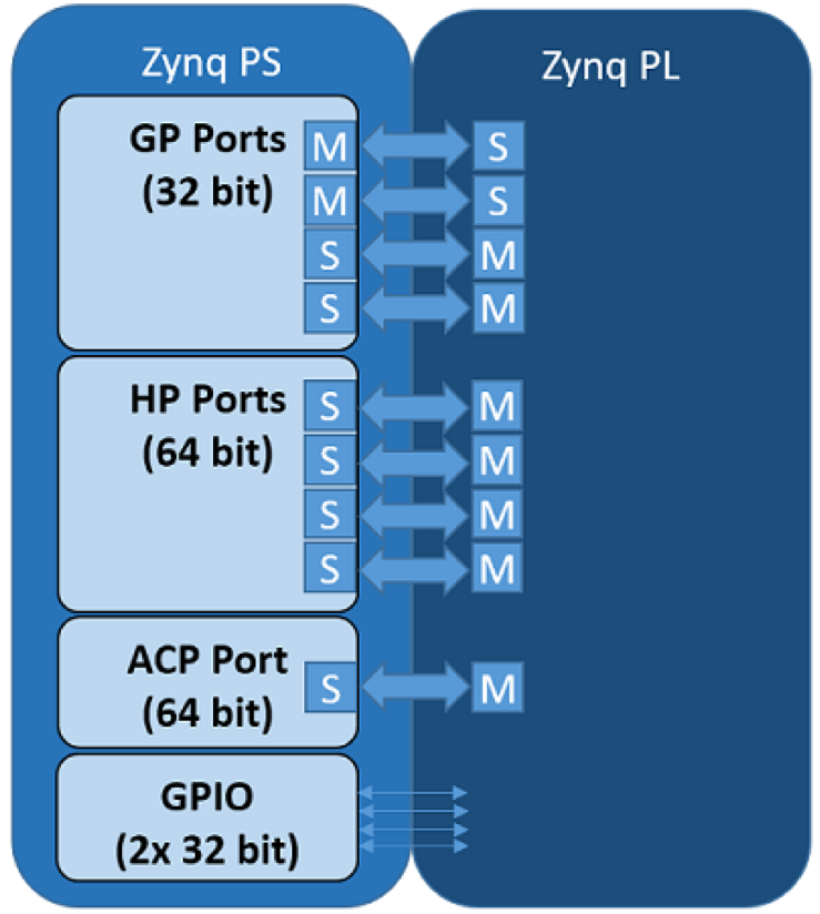
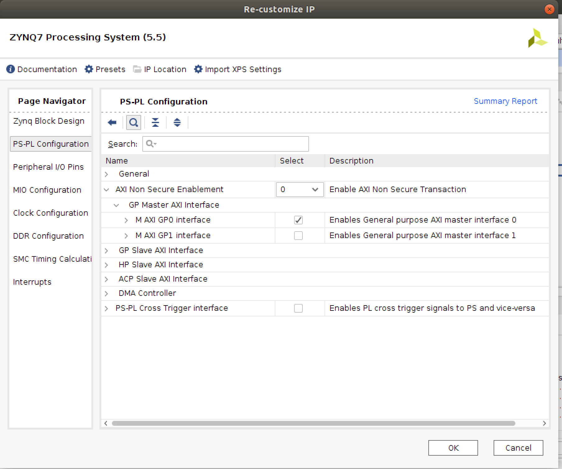
Chances are your Zynq processing system IP has already included that, but if it didn't open up your IP and then under the PS/PL tab, and under AXI Non Secure Enablement, ensure that a General Purpose AXI Master Interface (Pick GP0), is activated.
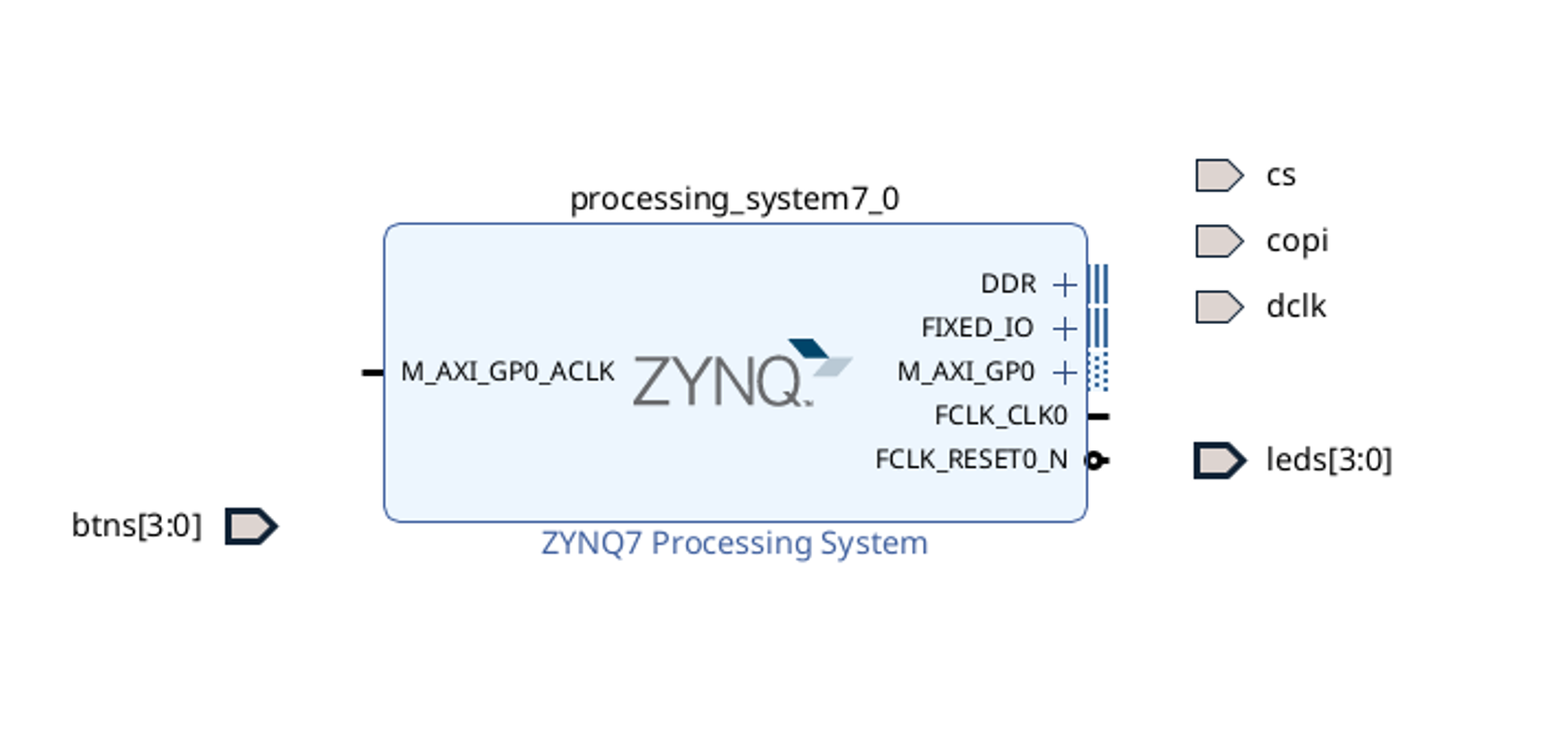
Afterwards (or maybe already automatically), your block diagram should look like the following:
Create a Piece of AXI IP
Now we need to build some IP that will interface with and AXI interface! Do the following:
- Go up to
Tools > Create and Package New IP - Click
Next - Select
Create AXI4 Peripheral - Call it whatever you want at the next window. I called mine
disp_interface, short for "display interface" but you do you. Feel free to have its location be adjacent to where your project is (likely in a folder calledip_repo). - In the next window that comes up it will show you a default module that has a single AXI4-LITE Slave Interface. That's in fact what we want here. We'll keep the defaults pretty much:
- The data width will stay at 32 bits (we can't change this actually since AXI-Lite requires 32 bits)
- Set the number of registers at 8. This will give you enough space to play with for this week's task.
- Click
Next - At the next window we're going to want to immediately go in and start editing our IP so click on
Edit IPwhich will now take us to our IP editor. What will likely happen is a second Vivado window will open up. This window will be behind your first one so it'll look like nothing has happened, so you may need to switch windows (remember the "U" in Vivado stands for "usability").
After you create your IP or if you ever need to edit it in the future, always feel free to right/control click on it in the block diagram view and then select Edit in IP Packager!
When you create IP in Vivado, it actually opens up a completely separate Project which you work in. When you are done, you package the project up into "IP". You can think of this as a compressed form of a project. You could, technically turn your entire Lab 1 project into a piece of IP if desired, for example...thus providing a means of abstracting layers of design.
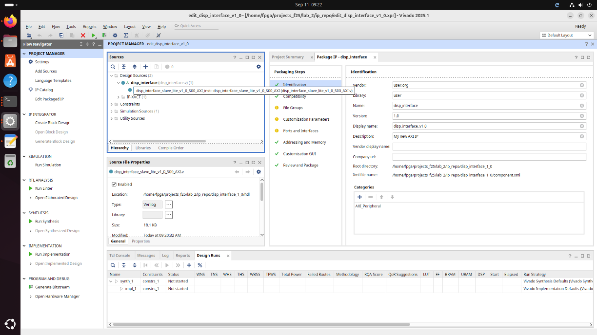
Once the IP editor is up, navigate into the sources menu and you will see a nested set of two Verilog files which represent your default AXI4-Lite Wrapper fitted to our specifications. Double click on the inner file (the outer one calls an instance of the inner one...the inner one is where the good stuff is at.) You'll note my IP is called disp_interface below (again you can name yours whatever, I'm just mentioning that for reference going forward).
This Verilog file, believe it or not, actually takes care of all the AXI-LITE timing and state machine handling for us! Study this file. The file has actually created a number of internal holding registers that have names like slv_reg0, slv_reg1, etc... These are each 32 bits in size and are the core of the data interfacing betwen the PL and PS in this example1.
OK so what should this module do? We've got eight 32 bit registers that we can use to exchange information between the PL and PS. We're going to use them roughly like so:
-
register 0 (
slv_reg0): this register will hold a hard-codeddeadbeefas a test value to read in Python -
register 1 (
slv_reg1): this register will hold the values of the four buttons to be read by Python (useful for inputs or debugging). -
register 2 (
slv_reg2): is used to specify whether we're doing a draw command (1) or configuration command (everything else) -
register 3 (
slv_reg3): contents to write.- If a configuration command, the
commandshould get set to be this value stacked twice (so{slv_reg3,slv_reg3}. - If a draw command, the
commandshould get set to a 64 bit command that uses these 32 bits to set the pixels in in the row specified in register 4 (below)
- If a configuration command, the
-
register 4 (
slv_reg4): second register for drawing. It will specify the row to be drawn to (refer to the MAX7219 datasheet for how to use these bits). -
register 5 (
slv_reg5): a trigger register. Nothing will actually get written or read here, but the act of writing to it by Python will be used to generate the trigger to run the SPI module.
We want to carefully and selectively modify this file (AND ALSO ITS WRAPPER WHEN APPROPRIATE DO NOT FORGET THIS!) so that we can "break out" this functionality. As of right now, the IP is set up to allow the PS (Python) to read and write those eight registers to it, but those values are not accessible outside the IP to the rest of the PL so we need to add those links.
Both the inner and outer files generated are VERILOG not SYSTEM VERILOG. That means you do not have the luxury of logic or always_comb, always_ff etc... You instead must use Verilog constructs of wire, reg, or always@(*) and always@(posedge clk), respectively.
In order to add links to the PL we need to add inputs and outputs to the IP Modules. Within both the inner and outer modules you should add the following inputs/and outputs (that will get interfaced to our SPI Controller):
  // Users to add ports here
  input wire [3:0] btn, //joe
  output wire [63:0] command, //joe
  output wire trigger, //joe
Data to the PS (from the PL):
Next, we want to set some values to be readable in Python. Towards the bottom of the file is a chunk of code that handles what data is sent back in response to read requests. The auto-generated code is a giant-one-line ternary. Breaking it up into multiple lines will have something like this:
	// Implement memory mapped register select and read logic generation
	assign S_AXI_RDATA =(axi_araddr[ADDR_LSB+OPT_MEM_ADDR_BITS:ADDR_LSB] == 3'h0) ? slv_reg0 :
	                    (axi_araddr[ADDR_LSB+OPT_MEM_ADDR_BITS:ADDR_LSB] == 3'h1) ? slv_reg1 :
	                    (axi_araddr[ADDR_LSB+OPT_MEM_ADDR_BITS:ADDR_LSB] == 3'h2) ? slv_reg2 :
	                    (axi_araddr[ADDR_LSB+OPT_MEM_ADDR_BITS:ADDR_LSB] == 3'h3) ? slv_reg3 :
	                    (axi_araddr[ADDR_LSB+OPT_MEM_ADDR_BITS:ADDR_LSB] == 3'h4) ? slv_reg4 :
	                    (axi_araddr[ADDR_LSB+OPT_MEM_ADDR_BITS:ADDR_LSB] == 3'h5) ? slv_reg5 :
	                    (axi_araddr[ADDR_LSB+OPT_MEM_ADDR_BITS:ADDR_LSB] == 3'h6) ? slv_reg6 :
	                    (axi_araddr[ADDR_LSB+OPT_MEM_ADDR_BITS:ADDR_LSB] == 3'h7) ? slv_reg7 : 0;
You're going to want to modify this portion of Verilog to provide information back to the PS. For example, since we always want the data at address 0 to be 32'hDEADBEEF regardless, changing it to this would achieve that:
	// Implement memory mapped register select and read logic generation
	assign S_AXI_RDATA =(axi_araddr[ADDR_LSB+OPT_MEM_ADDR_BITS:ADDR_LSB] == 3'h0) ? 32'hDEADBEEF :
	                    (axi_araddr[ADDR_LSB+OPT_MEM_ADDR_BITS:ADDR_LSB] == 3'h1) ? slv_reg1 : //put btn values into this one
	                    (axi_araddr[ADDR_LSB+OPT_MEM_ADDR_BITS:ADDR_LSB] == 3'h2) ? slv_reg2 :
	                    (axi_araddr[ADDR_LSB+OPT_MEM_ADDR_BITS:ADDR_LSB] == 3'h3) ? slv_reg3 :
	                    (axi_araddr[ADDR_LSB+OPT_MEM_ADDR_BITS:ADDR_LSB] == 3'h4) ? slv_reg4 :
	                    (axi_araddr[ADDR_LSB+OPT_MEM_ADDR_BITS:ADDR_LSB] == 3'h5) ? slv_reg5 :
	                    (axi_araddr[ADDR_LSB+OPT_MEM_ADDR_BITS:ADDR_LSB] == 3'h6) ? slv_reg6 :
	                    (axi_araddr[ADDR_LSB+OPT_MEM_ADDR_BITS:ADDR_LSB] == 3'h7) ? slv_reg7 : 0;
Interesting Aside
In previous versions of Vivado this auto-generated portion of code would get synthesized as a case statement (like shown below), which historically has always been the way to ensure you'd get low-latency multiplexer-based synthesized implementations of your selection logic. The fact that Vivado is instead default to generated a gigundous chained ternary for this behaviour means they must have significant faith in their synthesis engine.
	always @(*)
	begin
	      // Address decoding for reading registers
	      case ( axi_araddr[ADDR_LSB+OPT_MEM_ADDR_BITS:ADDR_LSB] )
	        3'h0   : S_AXI_RDATA <= slv_reg0; //replace with deadbeef for "sanity check"
	        3'h1   : S_AXI_RDATA <= slv_reg1; //put button values into reg data
	        3'h2   : S_AXI_RDATA <= slv_reg2;
	        3'h3   : S_AXI_RDATA <= slv_reg3;
	        3'h4   : S_AXI_RDATA <= slv_reg4;
	        3'h5   : S_AXI_RDATA <= slv_reg5;
	        3'h6   : S_AXI_RDATA <= slv_reg6;
	        3'h7   : S_AXI_RDATA <= slv_reg7;
	        default : S_AXI_RDATA <= 0;
	      endcase
	end
Anyways...back to the task at hand.
Data to the PL (from the PS)
A second thing we'd like to do is produce PL-side signals from register content. Since we're sending a 64-bit message to our SPI transmitter, we basically need to decide how to put stuff into that command out path that is correct. At the very,very end of the file is a region for user-added code. In that region I put something like this:
	//joe added code:
	reg [63:0] command_r;
    //gotta do this since need command_r to be reg for always block:
	assign command = command_r;
    //verilog way of doing always_comb
	always @(*)begin
        if (slv_reg2==1)begin //refer to register spec in lab!
	       command_r = {64'b0}; //change me!!!
	   end else begin
	       command_r = {slv_reg3, slv_reg3};
	   end
	end
Code like this enables the command signal to be based off of data written down into the various slave registers from Python. You'll need to finish that.
Another thing we want to do is cause a trigger from Python (basically position data in our our comman_out line and then from Python trigger a write. There's several ways to do that, but one way you'll often see in MMIO systems is doing a write event to a particular address.
Further up in the page in the code region where PS-side writing is processed, I'm going to add two little blips of code (somewhere in the line 200-ish range of the file):
First we need to make a reg to handle the trigger signal (same reason as the command_r signal above).
    //have to do this since want to assign trigger_r in always
    reg trigger_r;
    assign trigger = trigger_r;
Then inside the clocked-logic block that handles incoming AXI-writes, we're going to add some custom logic that sets trigger_r if a AXI-write event is happening, else not.
    //...around line 205ish...
	always @( posedge S_AXI_ACLK )
	begin
      //----------
      //add in this line which:
	  trigger_r = (S_AXI_WVALID)&&
	  	          (( (S_AXI_AWVALID) ? S_AXI_AWADDR[ADDR_LSB+OPT_MEM_ADDR_BITS:ADDR_LSB] :
	  	          axi_awaddr[ADDR_LSB+OPT_MEM_ADDR_BITS:ADDR_LSB] )==5);
      //---------

	  if ( S_AXI_ARESETN == 1'b0 )
	    begin
	      slv_reg0 <= 0;
	      slv_reg1 <= 0;
	      slv_reg2 <= 0;
	      slv_reg3 <= 0;
	      slv_reg4 <= 0;
	      slv_reg5 <= 0;
	      slv_reg6 <= 0;
	      slv_reg7 <= 0;
	    end
	  else begin
	    if (S_AXI_WVALID)
    //continuing on
The mixed indent-size is not my doing. That is Vivado's auto-generated code btw.
What this line does is basically set trigger to high when a write happens to register 5. It doesn't matter what is written, just that something is written. This is great, easy way to generate a trigger signal that fires for one cycle tied into a write action.
When you've made your changes (or what you think are the correct changes), go to the Package IP tab and click through each option and make sure they are green (you may have a non-critical IO warning about AXI CLK speed or Vivado telling you that the code it automatically generated for you is itself obsolete with what it wants...lol never change, Vivado...ignore these). The last one will be "Package IP" or something. Go ahead and click and it'll take you back to you main project.
If you made errors building stuff here, you can always return to this by recustomizing this IP from your main block diagram window. If you needed to make any changes (now or in the future) to your IP module, you'll need to always need to make sure you go through the repackaging checkmarks. This is important since it'll tell you what needs to be automatically updated, etc. For example a change in the Verilog file will require you to refresh stuff in the File Groups tab, and you'll almost always have to go the final Review and Package tab at the bottom and click on Re-Package IP.
Assuming you've built everything and all is good (and you've packaged the IP), it will ask if you'd like to return to your project. Click OK. If it doesn't and all is saved, you can just exit the IP project (but not Vivado overall).
Upon exit, it may also pop up a window about Generating Output Products. If that comes up, make sure to click Global, and totally and feel free to click on Generate. (you'll need to do that now or in the future).
Back in Block Diagram
When back into the main block diagram, add an instance of your new module. You should be able to just search for it by name under your IP entry field. (Mine was named disp_interface)
You should be prompted to allow the system to automate the AXI wiring. Click on that and let it do its thing:
I'd now add in your validated SPI TX that your wrote previously. Make a wrapper for your spi_tx just like before. Make sure it is verilog. One thing I did here is bury/hide the busy_out signal since we won't be using it. Also I made sure to invert the resest signal since the reset signal used globally with AXI is active low, but our reset is active high. This let's our spi module use the global reset.
module spi_tx_w(
     input wire clk,
     input wire rst,
     input wire [63:0] data_in,
     input wire trigger,
     output wire copi,
     output wire dclk,
     output wire cs
    );
    spi_tx  #(.DATA_WIDTH(64), .DATA_CLK_PERIOD(20))
    mspi
    (   .clk(clk),
        .rst(~rst), //IMPOTANT!!!
        .data_in(data_in),
        .trigger(trigger),
        .copi(copi),
        .dclk(dclk),
        .cs(cs));
endmodule
Add that module into your project and connect everything up. Notice I sliced the bottom four bits off of the command bus and put them on the led's to help with some debugging. If you haven't already let Vivado automatically wire the AXI stuff up for you. Note it isn't smart enough to wire up your modules like data_clk etc... so you'll have to do that yourself. When done you should have something like this:
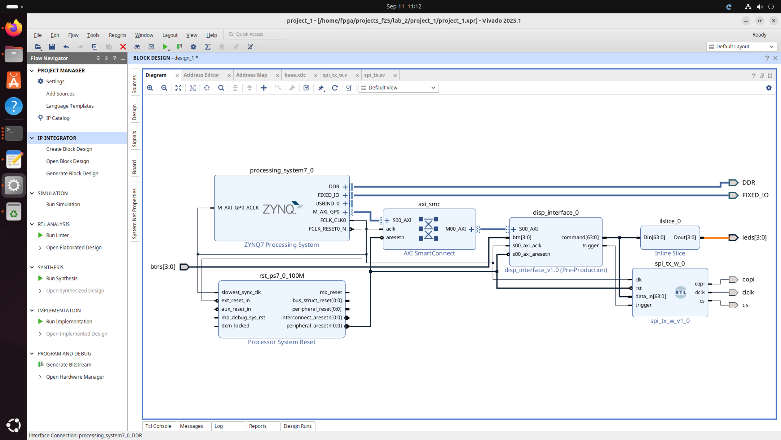
Depending on the order of operations from before you may get prompted about generating output products here (if you didn't earlier). The window looks like the following. It is very important that you make sure Global is specified~. You can also always just right click on the block diagram and tell it to generate output products too!
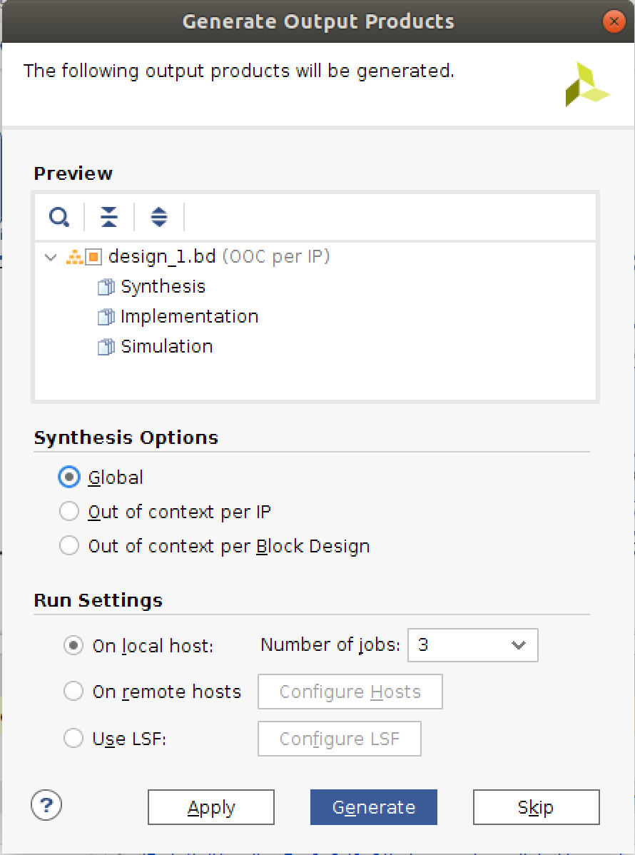
Just to reiterate, make sure to specify Global under Synthesis Options when it pops up. If you don't you'll get errors/critical warnings related to Out of Context Build issues later on. If you forgot to do this or can't remember you can always right click on your block diagram, go to Generate Output Products, change things and then click Generate.
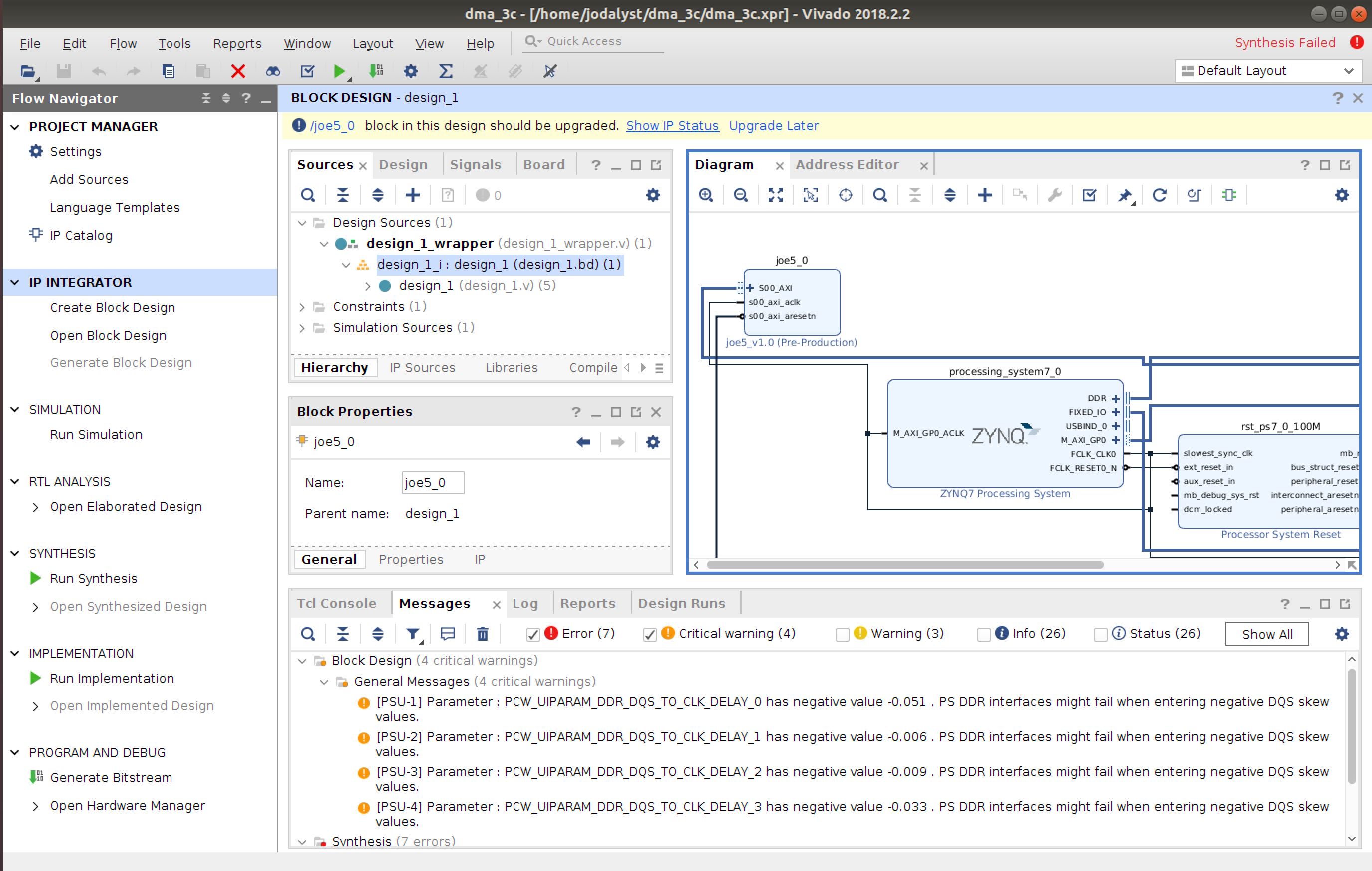
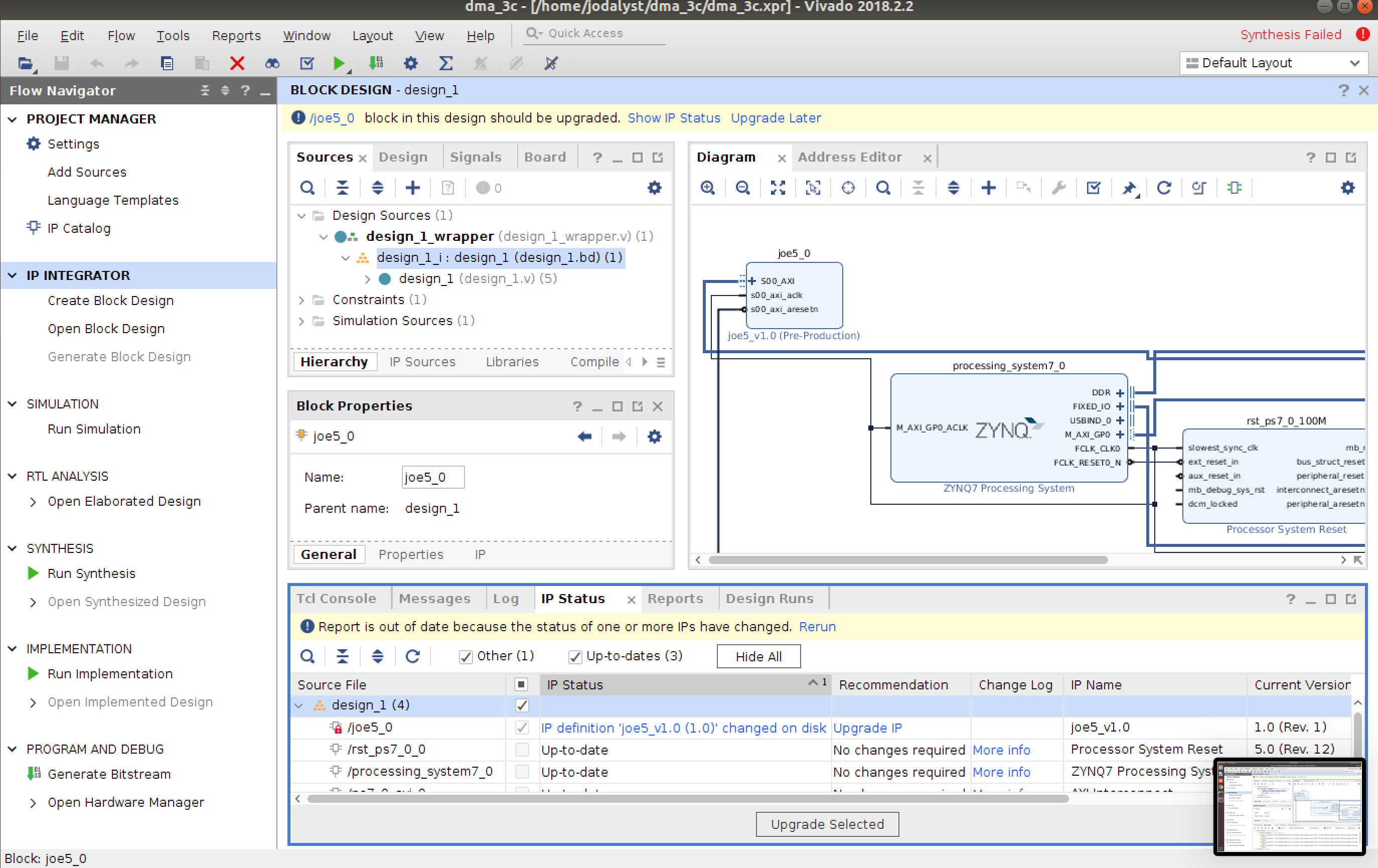
You are always free to go back and edit IP and stuff in the future, just remember at every step along the way just regenerate things (make sure Verilog is refreshed, saved, etc). Also note that if you go and update your IP at any point after having integrated it, Vivado will notice and prompt you to update/refresh all your IP. That will usually come up as an error, or a more friendly yellow notifier at the top. See the two images below:
Back on our main plot-line here, if all is good, verify your block diagram with the check-mark symbol.
Then right-click on your block diagram file, and go to Create HDL wrapper. If that builds fine, then save everything, and go to Generate Bitstream. AFter that it is completed (hopefully with no errors).
Interacting with it in Python
Ok deep breath...now hopefully things are maybe working...oh goodness.
Get your bitfile and hwh file up to your notebook just like last week. Make the new notebook and bring it in like we did last time:
from pynq import PL
PL.reset()
from pynq import Overlay  #import the overlay module
ol = Overlay('./design_1.bit')  #locate/point to the bit file
Assuming that loaded fine, let's do a thing we skipped last week. Run these two lines:
import pprint
pprint.pprint(ol.ip_dict)
What should pop out will be a massive dictionary that is basically the device tree of everything within your project. This is what that hwh (hardware handoff file) has been doing for us these last few times...giving the info to the pynq framework about what it needs. When I look at my stuff, I'll see a device labeled disp_interface_0 which is related to the name of my IP. I can access that piece of MM IP just by doing ol.disp_interface_0.
Then going into the Pynq docs, I can interact with this piece of IP using very basic commands like read and write while providing data. Try this simple script here. It writes some values to your registers and reads others. You should see some green LEDs light up on your board. You should also see data from those registers. One should be the hard-coded deadbeef, the other should be based on the four buttons you're pushing...make sure torun a few times with different button states to see what happens.
j5 = ol.disp_interface_0  #find the AXI MMIO module which we can talk to (name of IP)
#Now it is time to interface with the j5 IP:
# registers are four bytes in size, but address space is byte addressable! Keep in mind!
j5.write(0x08,0)  #write 0 to address location 0x08 (command type)..
j5.write(0x0C,5) #write "5" to address location 0x0C (should show up on green LEDs due to slice
j5.write(0x10,2) #write 2 to address location 0x10
d = j5.read(0x04)  # should read the value of all four push buttons (for test)
print(d)    #print output (hopefully buttons)
d = j5.read(0x00)  # read deadbeef hopefully (hard-coded in your mmio)
print(hex(d))
If the above isn't working as expected, there is little hope that the SPI is, so make sure above is actually working like you'd want!
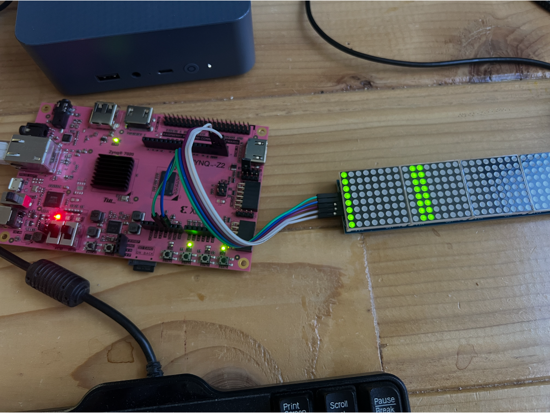
Now let's wire up the Display.
Connect the display to the following pins on the Pynq board (and do in this order):
- GND to GND
- VCC to 5V
- DIN to AR1 (the COPI line)
- CS to AR0 (the CS line)
- CLK to AR2 (the DCLK line)
Now let's interact with the SPI controller from Python. We set register 0 to 0, then send commands and write to the trigger register. When done the display should be ready to write to!
j5.write(0x08,0)  #write 4 to address location 0x08...which is register 2 (command type)
j5.write(0x0C,0x0F000F00) #display test command
j5.write(0x14,0x0) #trigger (write something to register 5)
j5.write(0x0C,0x0C000C00) #turn off display
j5.write(0x14,0x0) #trigger
j5.write(0x0C,0x0C010C01) #display on command
j5.write(0x14,0x0) #trigger
j5.write(0x0C,0x09000900) # decode mode 0
j5.write(0x14,0x0) #trigger
j5.write(0x0C,0x0B070B07) #scan mode command
j5.write(0x14,0x0) # trigger
j5.write(0x0C,0x0A010A01) #screen intensity set
j5.write(0x14,0x0) #trigger
The display hopefully flashed or at least dimmed a bit when the config commands were getting written. Now let's draw. The following example code will write three vertical lines on the screen:
j5.write(0x08,1)  #write 1 to address location 0x00 (drawtype)
for y in range(1,9):
    j5.write(0x10,y)  #write y to address location 0x08 (row address y indexed)
    j5.write(0x0C,0x00000601)
    j5.write(0x14,0x0) #trigger
If it ran fine, you'll get a pattern like this:
If not...well better head back to the design and figure out what went wrong. One thing you may want to do is make sure you are actually triggering SPI writes. A logic analyzer or an oscilloscope may be helpful here.
Eventually you'll get it working though. I believe in you. This is getting sweet...you can smell the layers of abstraction piling up. And they smell good. In the field (or your final project), you could now imagine that you could perform a complex operation in the hardware quickly (let's say a Fourier Transform on some audio data, and then extract certain peaks and report them back, and have all of that wrapped up in a nice little function that anyone could use.)
Finishing Up
Do something with the display. Make an animation or a game or something. You have access to the buttons via register 2, so you can take user inputs. Or make an animation. You're doing all this in Python, so I don't want to hear any complaining. Maybe make a smiley face that frowns when you push a button...something. Programming won't get any easier than that until AI takes all our jobs in eighteen months or so.
.v file (the product of all the block diagramming),file.

Show your working MMIO system to a staff member.
Lab initially inspired by video here
Footnotes
1remember in lecture 4 how I said Xilinx/AMD really use Master/Slave terminology a lot...this is another example of that. All the auto-generated stuff doesn't even just use M/S prefixing but "slv" as you can see. Hence, we'll just roll with it to avoid adding an extra layer of confusion on us.