Introduction to PYNQ
Python with an FPGA? No Way
Please Log In for full access to the web site.
Note that this link will take you to an external site (https://shimmer.mit.edu) to authenticate, and then you will be redirected back to this page.
In this lab we'll build up a basic "full" Zynq system that contains both the Processing System (PS) and the Programmable Logic (PL). The final result should be something like the video below, which shows a system which takes both physical buttons and computational inputs. It is a low-pressure, relatively first-splash experience of the whole pipeline that we'll be using a lot this term.
Prior to Getting Started
Because we'll be working on both the Processing Systemt ("PS") and with the Programmable Logic ("PL"), we're going to need to make sure you have the system all set up in regards to the Pynq Board Image that will go on the SD card. Please grab a microSD Card that is pre-flashed with the appropriate PYNQ framework on it (there should be a labeled box at the front of class or ask Joe or Kiran). This microSD card will be yours for at least the first few weeks so you should keep it with you and remove it from the Pynq board when done (since we'll be keeping the boards in the lab room for now. Don't put it in yet. We'll do that later.
You can worry about booting the Pynq up later. Let's do some designing first.
Getting Started
We need to open up Vivado in Project Mode, this means using the Graphical User Interface. Deep breath. Previously in 6.111 we built our projects in non-project mode which actually resulted in slightly longer build times since the system wouldn't cache the design in stages, but did allow us to keep a much, much lighter-weight file structure. For the sake of working with the Zynq we will be working in Project Mode. For right now, just roll with it. Later in the semester, in particular before we hit final projects, I'll give you some tcl scripts to help you work with Project mode in a way that allows for version control.
- Launch Vivado from a terminal by just running
vivadowith no other arguments. (if that doesn't work for some reason, the binary is under/tools/Xilinx/2025.1/Vivado/bin/vivadoon our lab machines. Either way the GUI will open up. - Click
Nexton Create a New Project - Name it something you'll remember like
led_controller_1or something and clickNext - Select it as an RTL Project and click
Next - Don't worry about adding Verilog sources right now so click
Next - Add the `base.xdc file found here (and make sure to specify "Copy Constraints File Into Project")
- When prompted to choose a device do one of the following (and after that click
Next):- Go to the boards page and choose the Pynq Z2 board (if that file is installed...it'll probably show an image of the Pynq Board...and it should be installed if you're on a lab machine...if you're working on your own personal Vivado install, you'll want to add the board files. Email me or post on Piazza and I'll show you how.). This is the preferred method since it will associate some important other constraints with your project that have to do with timing issues.
- if the board isn't already there: first click the "refresh" button, then search the boards for "pynq", and click the "download" looking icon under the "Status" column. This should make the preview picture of the right board load in.
- Go to the boards page and choose the Pynq Z2 board (if that file is installed...it'll probably show an image of the Pynq Board...and it should be installed if you're on a lab machine...if you're working on your own personal Vivado install, you'll want to add the board files. Email me or post on Piazza and I'll show you how.). This is the preferred method since it will associate some important other constraints with your project that have to do with timing issues.
- Click
Finish
Some stuff will fly by and then boom, you'll be in the project mode. Right now there's only one file, your xdc, which you can see in the upper left side Sources manager. We need to add more. Let's do that.
Starting Our Block Diagram
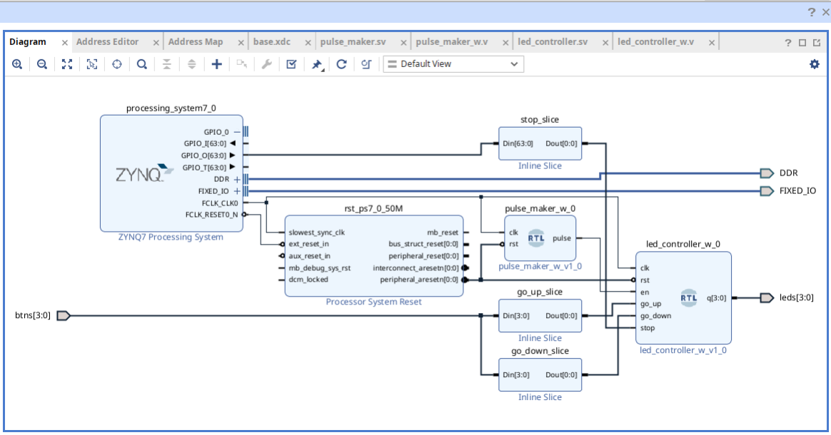
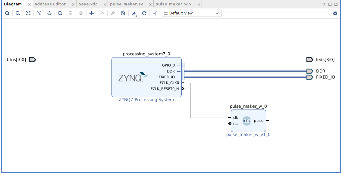
We want to eventually build this block diagram of our system:
If you're coming from 6.111/6.205, this would be the point where we create/add a top-level Verilog file. (we'll eventually do that but we'll have Vivado generate it automatically from what we're about to do here). We'll instead go the block diagram route for now because AMD/Xilinx Vivado really, really wants you to use the graphical pipeline for doing anything with Zynq products. It is not ideal, but it isn't as bad as I made it sound in lecture. Just don't expect amazing things from it. Start with low expectations and then, no matter what, you'll be happily surprised.
Activating and Configuring the Processor
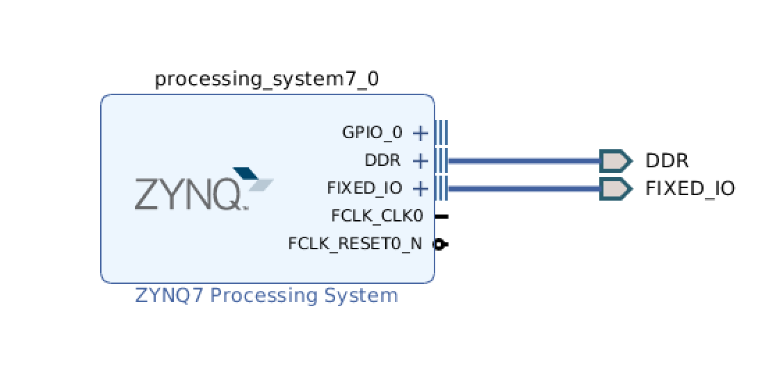
We first need to make a design entry point for the processor on the system (remember there are ARM cores on this board)....something that let's us customize and modify the Processing System ("PS") and will then allow us to link things we design in the Programmable Logic (the FPGA part) (the "PL") to it.
-
Under IP Integrator on the Left side, click on
Create Block Diagram. Call it something you want (I usually just dodesign_1, but you do you). Keep file locations as the defaults and/or locals -
A blank
Diagramwindow should appear to the right. It is blank and we want to eventually fill it so that it will look like the first image above (our final system for this lab). To do that we're going to add IP and modules. We're essentially doing what we've always done in 6.205 with straight-up Verilog, but instead we'll be doing it graphically and this can help in a lot of ways. -
Add a piece of IP to the design by clicking on the
Add IPbutton (or press control-I). -
Search for and add the
ZYNQ7 PROCESSING SYSTEM. Click on this. -
After it is added, you should almost immediately see a green option window at the top that says
Run Block Automation.- Often times Vivado will suggest things to connect for you. Be careful with this since it is stupid sometimes, but really helpful other times. This first one, we can just trust it, so let it do its thing. Click on it.
- In the window that pops up, it'll tell you what it is trying to auto-connect. Always review this! It'll say something about making DDR and Default IO external for us. This is good. Let it do that. Click
OK - Some new wires should appear as well as some
External InterfaceslabeledDDRandFIXED_IOwhich correspond to output pins (a subset of the output pins can be accessed by the PL, and a subset can be accessed by the PS)
-
We now need to customize the Zynq PS for our purposes. Big picture, for this first lab we really want the ability to just "share some bits" between the PL and the PS. There are many ways to do this from very structured ways using AXI ports, to large-data-throughput ways like direct memory access. For now we'll just do a relatively low-throughput connection (GPIO).
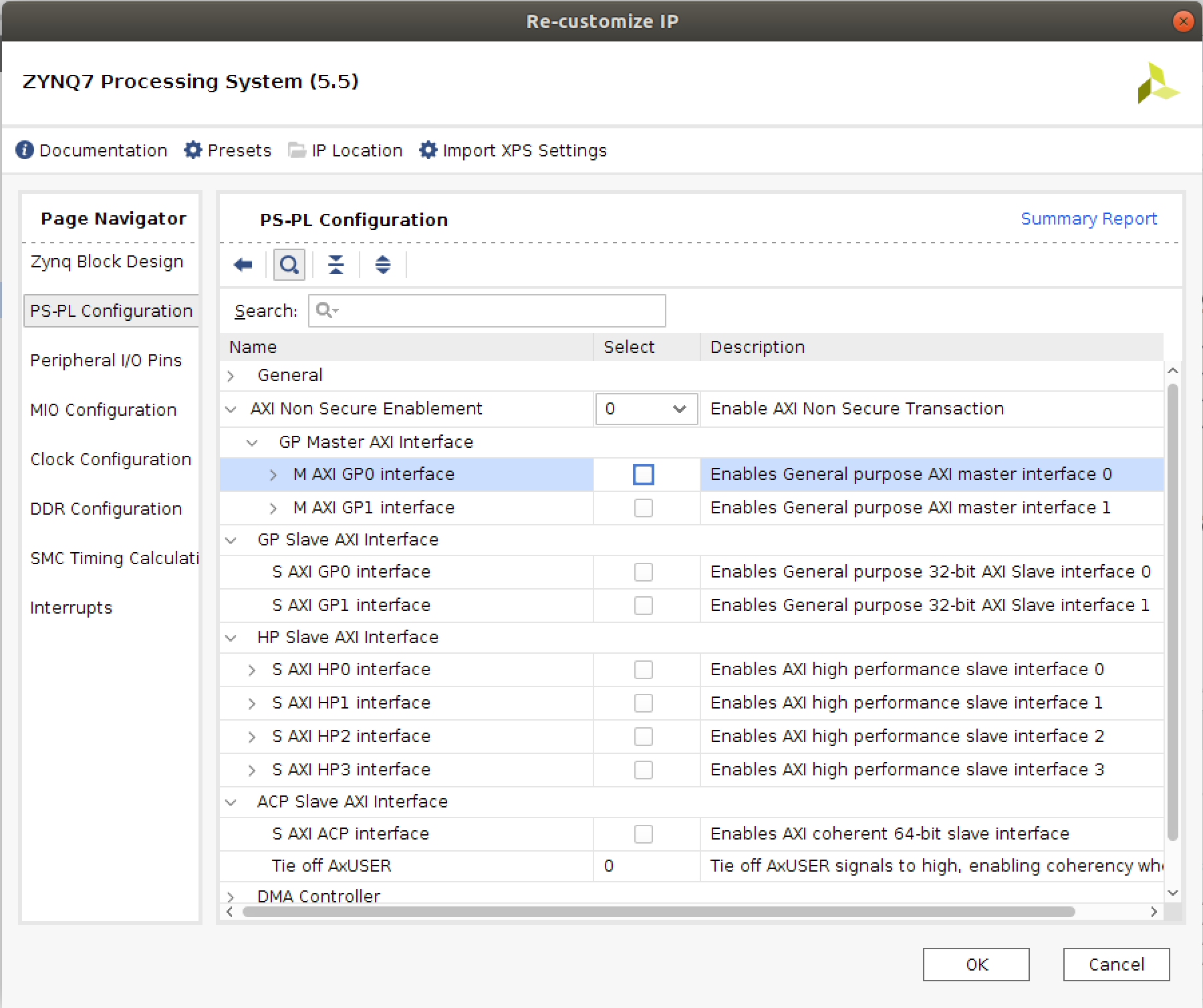
To do this double click on the module. First off we're going to disable the AXI ports that connect the PS to the PL directly. (We'll use those later in other labs or in projects). Go to the PS-PL configuration tab and make sure no options are checked (including under any submenus). They will probably already be unchecked, but double check. Sometimes, some default setting gets wonky. It should look similar to below:
- Next we want to enable some "General Purpose Input Output" (GPIO) pins on the PS. To do this click on the
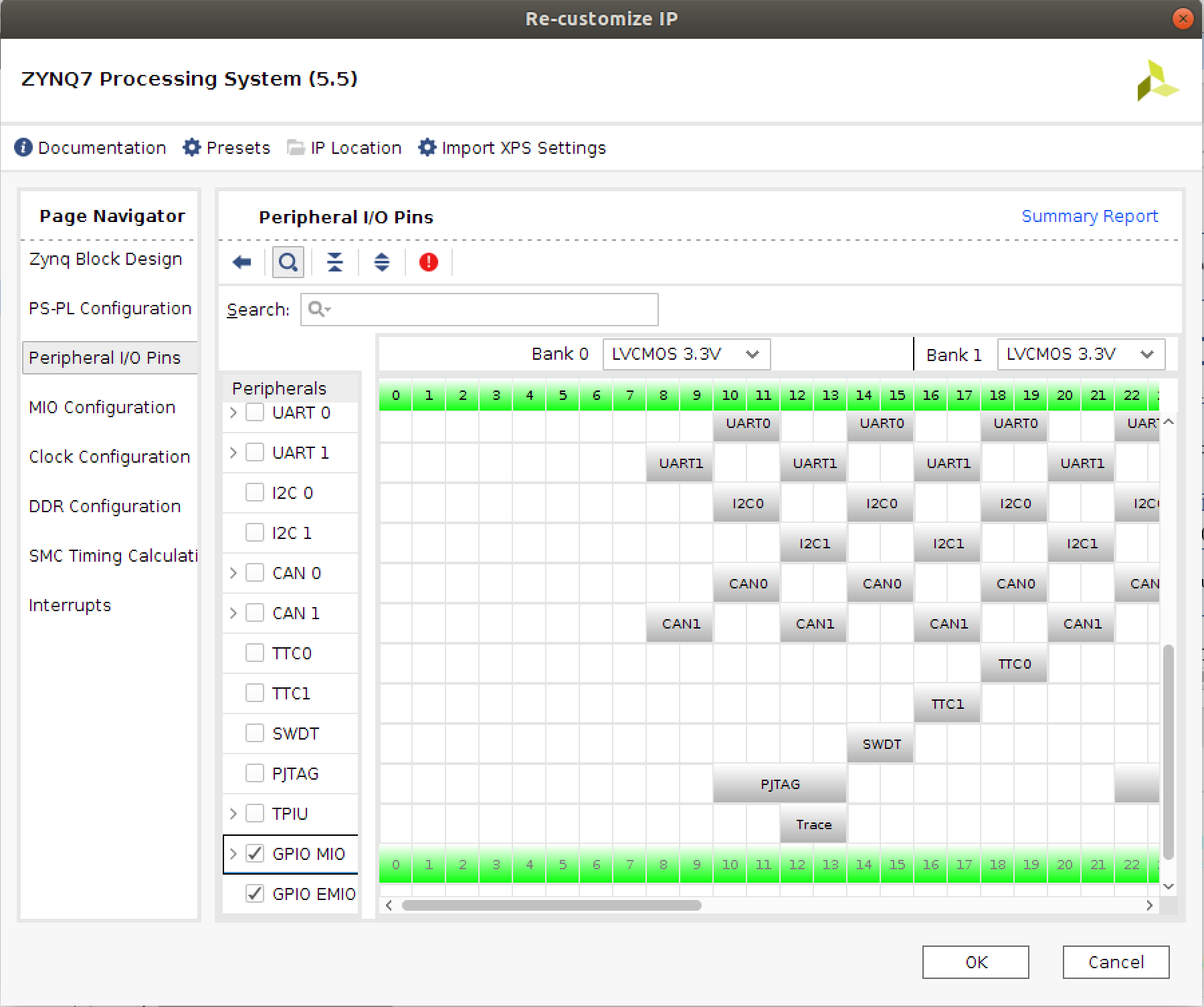
Peripheral I/O Pinstab and scroll to the bottom, selectingGPIO MIOandGPIO EMIOlike shown below (you'll note the pins will turn green indicating they are in use) At the same time make sure to disable all other uses for these pins (Flash SPI, UART, etc.)
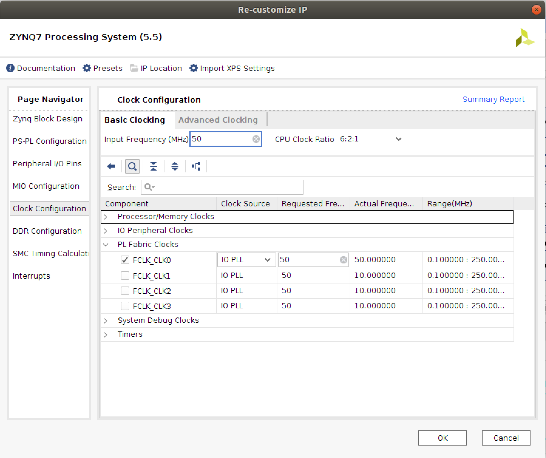
- Finally let's enable a clock of a particular frequency. Zynq systems have a number of clocks that run in the PL, but which are configurable and controllable from the PS. This allows the software side of things to vary the speed of logic implemented as needed (and this can be done with very simple python API calls since it is really just nudging a single MMIO mapped register). Some more info here. Go to the
Clock Configurationtab and underPL Fabric Clocks, selectFCLK_CLK0and set it to generate a 50 MHz frequency like shown:
- When the above three things have been done, click on
OKand the Zynq system will update itself (some pins will appear, others will disappear). It should look like the following when done. You'll likely get a warning about someDDR_DQS_TO_CL_DELAYs having a negative skew value of something like 50 picoseconds or so. Dont' worry about that. Otherwise, make sure it matches, since unused pins may cause issues:
Adding Our Own Interfaces
We now want to interface to some outside connections that the PL is connected to. In particular we want to interface to the buttons and to the LEDs on the PYNQ board.
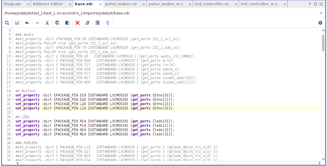
- Open up your
base.xdcfile (find it underSources>Constraints) and make sure that everything is commented out except for the set of lines referring to the LEDs and the buttons. Depending on the version of your XDC, they may have different names. Plurality and Capitalization matter so pay attention to what they are called. Your XDC should look similar to below (make sure to save the file):
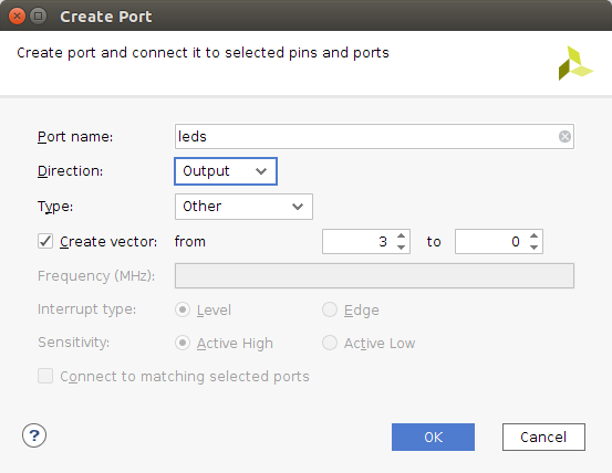
- Next, go back to the block diagram, and
Right Click > Create Portor press Control-K. This will bring up the option to create inputs and outputs to the PL. Create two ports, an input for the buttons and an output for the LEDs. Should make sense:- Create one with the exact name of your LED pins. Make it an
Outputand aVectorfrom3 to 0(since there are four LEDs) - Next create another port with the exact name of your button pins. Make it an
Inputand aVectorfrom3 to 0as well.
- Create one with the exact name of your LED pins. Make it an
When all finished, you should have an input and an output port.
As you may remember from 6.205/111, the XDC file maps the cryptically named pins on the FPGA (names like D19 and R14 which express position in the ball grid array) to meaningful names that we can use in our designing. When building the bit file up, Each active pin also requires some setup/interfacing to be built around it so make sure to only uncomment pins that you're using otherwise you'll make your build times unnecessarily long (and they are already long as it is).
Integrating Verilog Modules
We now want to create two modules in Verilog. The first module will be a pulse generator (it takes in a clock and generates a periodic event from it. Nothing crazy. Should be EZ to do since you've done 6.205...in fact we'll just give it to you as a warmup).
To make a new module go to PROJECT MANAGER >> Add Sources >> Add or Create Design Sources, and then Create File. Name it whatever you want (maybe pulse_maker.sv is a good one, just keep it local to your project and avoid spaces in the name, otherwise it'll be hell. Finish and then move on. Vivado will then try to "help" you by allowing you to declare the Verilog module you want to write inside this creation GUI. Just skip this part unless you like wasting time. You can type it out way faster.
Here's the source...assuming the clk is 100 MHz (not necessarily true, this will fire 5 times per second). Note the reset signal is active low. This will be more compatible with the default on the system (see that in a minute).
`timescale 1ns / 1ps
`default_nettype none
//will fire a pulse once every 20 million clock cycles
//feel free to change/modify
module pulse_maker( input wire clk,
                    input wire rst,
                    output logic pulse
    );

    logic[31:0] counter;
    localparam PERIOD = 20_000_000;
    always_ff @(posedge clk) begin
        if(!rst) begin //active low reset just for fun
            counter<=32'd0;
        end else begin
            if(counter==PERIOD-1)
                counter<=32'd0;
            else
                counter<=counter+1;
        end
    end
    assign pulse = (counter == PERIOD-1); //feel free to change this later.
endmodule

`default_nettype wire
Add this code into your SystemVerilog file. Save your code.
It is at this point where you've probably just used Vivado's built-in editor. For copy-paste and/or uncomment jobs it is fine, however once you start needing to write from scratch or seriously work with stuff, you may find it frustrating. For now, let's just use it, but at the end of this lab, we'll talk a bit about the Vivado project file structure, where the actual important files are, and how you can edit in an external editor.
Now here is an annoying part. Vivado's Block Diagram Editor will not permit the integration of SystemVerilog files into it directly. I honestly don't know why. This was an issue seven years ago and I thought it was a feature they just didn't get to yet, but they've never gotten to it and they don't seem to have any intention of supporting it. In their defense there are probably some legit reasons for it given that supporting SystemVerilog means having to support a lot of other interesting things like interfaces so I do kinda get it, but it is annoying. Nevertheless, how do we integrate SystemVerilog into the project? By wrapping it in Verilog. No joke. That doesn't even seem like it should be legal tbh. It is like when gmail blocks you from sending a python file because it thinks it is malicious so you just change the extension to .txt and it gets right through the filter.
Make a new file and call it pulse_maker_w.v (the w stands for "wrapper"). In that, make a "pass-through" module that literally has the same inputs and outputs as the actual pulse maker module you wrote above. This wrapper module should have an instance of the pulse_maker in it. It'll look like this:
`timescale 1ns / 1ps
`default_nettype none
module pulse_maker_w(   input wire clk,
                        input wire rst,
                        output wire pulse
    ); //pure verilog does not have logics only wires.

    //instance of pulse maker:
    pulse_maker mpm (
        .clk(clk),
        .rst(rst),
        .pulse(pulse));
endmodule

`default_nettype wire
OK Now this is what we'll integrate into the design.
Assuming you have a working module, we now need to integrate it into the block diagram. To do this:
- Right click on the background of your block diagram and click on
Add Module. Select yourpulse_maker_wmodule and it will appear! - Drag the module to somewhere convenient
At this point you can potentially run some connection automation (it will likely prompt you at the top). If you do that, the system will attempt to wire the fabric clock from the Zynq processor to the pulse_maker_w input. In the process it'll add a clocked reset module. You can either let it do this or skip the clocked reset module and wire the Zynq Processor clock to the pulse maker clock and its reset to the reset of the pulse maker manually. It is up to you. For this lab it won't matter. If you don't let it automate/do it manually, you'll get a warning about an asynchronous/non-clocked reset signal, but you can ignore it. In more complicated designs you should probably let it do its thing here.
What the Processor System Reset does is allow you to fire a reset signal from your ARM cores into your FPGA fabric when you do things like reload files or the entire image we'll be running eventually. The module synchronizes the signals from the one domain into the other for widescale use.
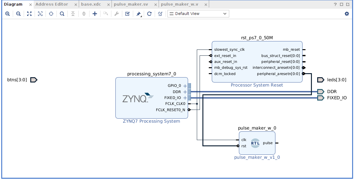
- Vivado likely used A.I. to determine that your
clksignal needs to connect toFCLK_CLK0andrstto a signal derived fromFCLK_RESET0_N. It usually is pretty smart about this stuff, but always check these things. It can mess up, especially if you have poor naming, and once we get to lots of clocks, etc... If you don't let Vivado automatically connect your pulse maker, connect the fabric clock to your clock input and the Zynq reset to the reset on your pulse maker module. You can connect stuff by hovering over the port/input/output of interest on a module and a little pencil symbol will appear. Click and drag/move your mouse to where you want to connect it. It'll snap and auto-route for you.
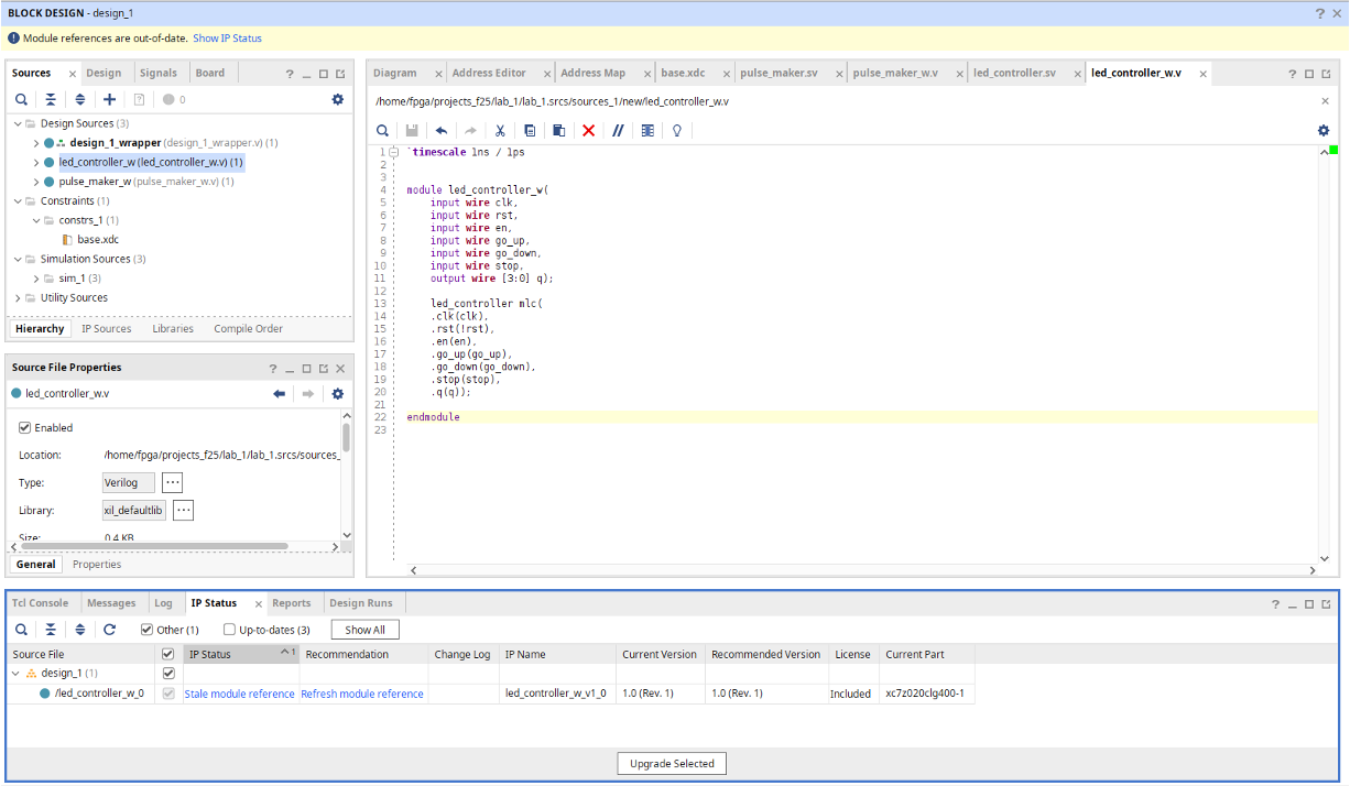
LED Controller
OK the LED controller you made in the previous assignment will be the next piece we need to deploy. Thankfully you've already thoroughly verified it using simulation, right??? You should be able to then just drop it into the design.
However you want to do it, add a copy of this file to your project as we've done earlier. Whatever you do make sure you tell it to make a local copy when creating.
Remember, though we can't just integrate this module in directly since it was written using some SystemVerilog constructs. Instead we need to wrap it in Verilog like we did for pulse_maker. After that drop it into your block design and and wire its four bit output (q I believe) to the LED external interface. This should be no problem. Also connect the clk and rst signals to the global signal paths in the design, and connect en to the output of the pulse_maker module (so that way your led_controller module will step at a very visible rate of once every 400 ms or so).
For the three remaining controls on led_controller we're going to do the following:
btn[0]should get connected to thego_downsignalbtn[1]should get connected to thego_upsignalGPIO_O[2]from the processor should go to thestopsignal
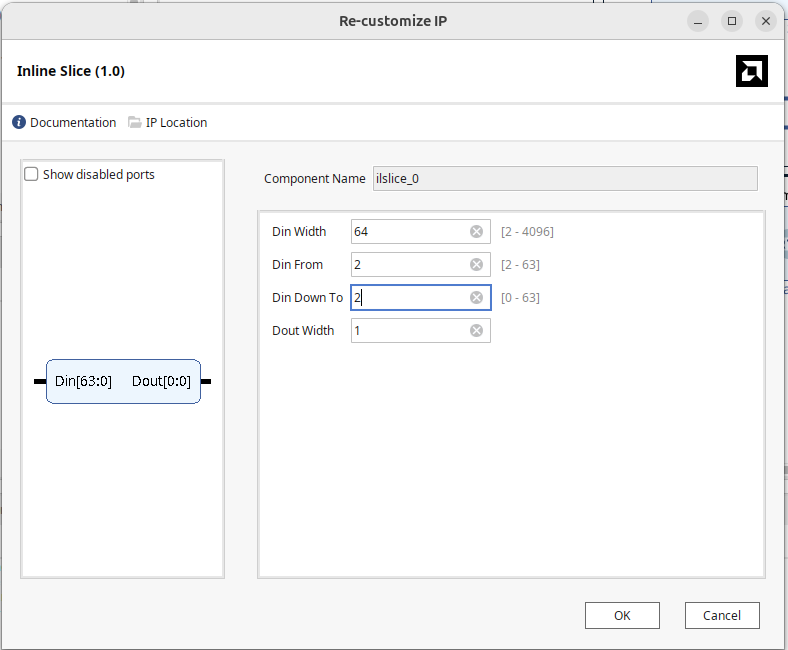
If you just try to make the magical GUI wires connect it'll have issues since there are different bit widths. Each input pin on the this module is one-wide whereas the buttons come in as a four-wide vector, and the GPIO out from the Zynq processor is a 64-wide vector. This will cause issues. Damn. Well there is a solution. We could actually just write some Verilog modules to handle this. That is one solution. However there is already IP for this believe it or not...they're called Inline Slice modules. We can use some Inline Slice modules to select/de-mux down. To do this go to the Add IP window and search for Inline Slice. Add one and double click on it. We will need three Inline Slices:
There are also "Slice" IP's which do effectively the same thing but they got deprecated in 2025 and replaced with inline slices. So use the inline ones, even if I typo and only say "Slice".
- For the one that slices the Zynq PS GPIO, make its input width (
Din) be 64. Then make bothDin FromandDin Down Tohave a value of 2. This is telling the slicer to take in all 64 values and only put out value on pin 2.
- Make another slicer that slices the four button
btninputs down to 0 to 0 (forgo_down). - Make another slider that slices the four button
btninputs down to 1 to 1 (forgo_up).
To connect to the GPIO pins, hover over them and a down-down arrow symbol will appear. Click this to expand out the GPIO OUTPUT, INPUT, and T pins (used with high-impedance paths). Then connect to Output!
You can name your Inline Slicer (or any module) through the Block Properties box that should come up when you click on it. Name your one coming from the GPIO thing, stop.
Run the appropriate wires/connections between all these modules. When completed you should have a system that looks like the following (shown earlier, but again here for clarity)
Double check that things match up! If you let Vivado wire up your pulse_maker automatically, you'll also have a reset module in there. No worries either way.
Note if you already have Verilog files written somewhere else, you could be importing them at this point. Regardless, makes sure you always keep copies of the actual files in your project directory and just let Vivado manage it. Otherwise, you'll maybe get weird errors/permission issues.
Putting It All Together
OK if everything is good so far, you can do a couple things:
- Click on the
Optimize Routingbutton (search for it...it is like a twirly arrow and a right-angle-step wire) in the top bar of the Diagram window. This will clean up everything for you (and generally does a good job at it). - Then click on
Validate Design. (check mark symbol) This will do a first-pass (very surface-level) sanity check of your system and flag any potential problems (unconnected wires, incompatible pins, etc). Depending on if you added the reset module or not, you'll get one warning about an asynchronous reset. For this lab, don't worry. If you get other warnings/issues, read them through. They will be telling you information! Adjust your design accordingly. - If all is good, under the
Sourcesmenu, right click on the block diagram file (the .bd file which has a symbol that looks like a stack of gold bars), and click onGenerate Output Products. This will generate some important linker files, including the important hardware handoff file we'll need to use in a bit. - In addition, if still no issues, under the
Sourcesmenu, right click on the block diagram file (the .bd file which has a symbol that looks like a stack of gold bars), and click onCreate HDL Wrapper. Let Vivado manage this thing for you. In the future maybe you will manage it yourself, but we're not there yet emotionally. This will create a high-level Verilog file for us/converting the block diagram into it. - There should now be a
design_1_wrapperthing in the sources tab on the left. Make sure that is BOLD with a three-box-green-on-top-box symbol. If not, right click on it, and click on "Set as Top". This is how we tell Vivado that this is the entry point of our project. Previously when doing tcl scripts, there'd be a line that specifies this, but we need to do it here. Wait for a bit while things flash and it should appear bold now. If you double click to expand it, inside there will be something nameddesign1.v. This is actually the source file for you design. This is a standard Verilog file made from your block diagram. It should, for the most part make sense, and if not, at least be familiar looking. This really is the goal/dream/intention of this block diagram thing...automating a bunch of annoying module instantiations....now back to the journey. - If still no errors pop up, then go and click on
Generate Bit Stream. This will start the whole build process of Synthesis, then Implementation, and then Generating the Bitstream. Depending on your computer, this could take a couple minutes for this project (and potentially longer if you forgot to comment out unused things in your XDC). Errors could appear at any point in this build process so pay attention to the error logs and ask for help if needed. They will appear in the bottom terminal thing. Make sure to have Errors and Critical Warnings and Warnings visible. As we've seen in 6.205...Errors are really bad. Critical Warnings are usually bad, but sometimes fine. Warnings are often ok, but can be symptomatic of issues. - Cross your fingers while it runs.
- If errors come up as it builds, note what they are and either ask for help, or look them up.
Moving it to the Zynq PS
If everything went ok in the previous section we need to move two files to your Zynq over the network. These files will live inside of your project folder for what you were just building. Assuming your project was called cool_project and your block diagram was called design_1 you'll find:
design_1.hwhincool_project/cool_project.gen/sources_1/bd/design_1/hw_handoff/design_1.hwhdesign_1_wrapper.bitincool_project/cool_project.runs/impl_1/design_1_wrapper.bit
We need to copy both of these files over to the Zynq file system now. So this brings us to actually powering up the Zynq board. Let's get started.
Getting the Zynq On
You should have a microSD card that will be your Pynq OS.
- Make sure the Pynq board is powered off.
- Insert your microSD card.
- Power the Pynq on. It will take maybe a minute or so. When done booting, it will flash some on board LEDs and the "DONE" LED will be green.
We now need to get onto the Pynq board. You'll notice it is connected with an ethernet cable. That gives it network access and it should be accessible in that manner. We've set up mini router networks for all Zynq stations in the lab. In those stations, the lab computer is also on the network (and if you'd like your computer can get on the network too by using an ethernet adapter. We can't do wifi since all the little wifi networks will jam eachother so wired it is going to be).
Anyways from either the lab computer or your laptop on the network you should be able to go to your router at your station's IP address (like 192.168.0.1) and under there you should be able to see what IP address your Pynq board has taken. Often times it'll be 192.168.0.101.
In a web browser, visit that IP address. It'll prompt you with a login. Username and password are both xilinx. Afterwards you'll get something like this:
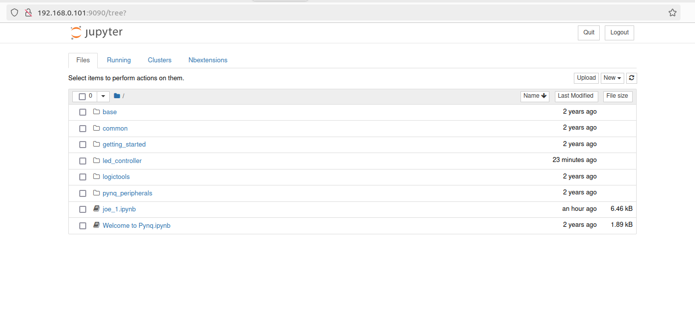
This is a Jupyter environment hosted on the processing cores of the Zynq board. Kinda cool. Anyways inside of this let's make a new folder for this project. You can see in the image above I made one and called it led_controller. Move into there and create a new notebook. We'll use that in a minute.
Also in that folder, we need to upload the two important files we talked about earlier. There should be an upload button. If you're doing this on the machine that did the builds, you can navigate in that to get the two files up. I renamed them led_c.hwh and led_c.bit, but you can name them whatever once they're inside. Just make sure they have the same base name!!! That is important.
As an alternative, if you're a cool kid, which you all are, you should just scp these files up from the lab machine to the Zynq OS no problem too. Doing something like this from the lab machine will put the hwh file into the base jupyter notebooks folder on the zynq os (note password to do this is xilinx).
scp design_1.hwh xilinx@192.168.0.101:~/jupyter_notebooks/
I know this can be confusing if you've not done this before (I've been there, please believe). Feel free to ask for help about this or post on Piazza or something. Once you get the hang of it, it is fine, but before it can seem daunting.
If these got placed on the machine with no errors we now need to go to the Jupyter Notebook to do something with them.
Running it on the Zynq PS
We can interact with our system via Python using two different methods. The first is you can just ssh into the Pynq board, and write a Python file and run it right from the terminal. If you're comfortable doing that, then great. I tend to do this since I wasn't raised on Jupyter notebooks, but I gotta say I do see the point of Jupyter notebooks and that approach so totally go with that if you'd like. The Jupyter notebooks also allow an easy way to get some graphical feedback.
If you do the Jupyter approach, in a web browser (on the same network as your router that the Zynq is connected to), type in the IP address of your board. It'll prompt you to log in. Again, the password is xilinx. When there, feel free to make a new directory and/or move folders and files around. I made a directory called led_counter and put the ledc.hwh and ledc.bit file into it. Then I moved into that directory and created a new Python3 notebook.
Into that notebook I put the following chunks of code and ran them in sequence:
The first one is the following:
from pynq import Overlay
ol = Overlay("./led_c.bit")
This code imports the Overlay library which we then use to load the bit file we just generated. When you do this, the library looks for the similarly named hwh file, which should be located in the same directory (you moved that in right?). When that gets done and checked, you should be good to move on. If you run this blob, you should see an LED come on (but probably not be visible sweeping left or right). If you push Button 1 or Button 0 you should get a scrolling action going...but do you?
An Error (Possibly Optional If You Were Really Sharp Earlier)
Chances are (I did this actually so it is a pure true organic error), your LEDs aren't dancing when you push buttons 0 or 1. This is likely because you/I/we forgot that the rst signal on led_controller is active high, but we fed it an active low signal. So what is likely happening is your system is stuck in reset (and led[0] should be stuck on).
We need to fix this.
The cheapest/easiest way to do this is probably just invert the reset signal before it hits the led_controller module. One benefit (perhaps the only benefit) of having these wrapper modules (.v files) is that you can do very easy/quick signal modifications like this into and out of your .sv files which then lets you leave your verified designs untouched. For something like this, it might seem silly, but for larger changes down the road, this layer of isolation is nice.
So I just inverted the signal inside led_controller_w on the way into led_controller as shown below:
As soon as you do that, though, you'll notice a little yellow "you changed stuff" warning comes up. This is good, because it is telling you that your modules/IP in the top level are now out of date so you need to regenerate. Check out the IP status, then Update the ones it says are out of date. That will also likely prompty you that you need to regenerate output products...let it do that. Once that is all stable, then go and do anther Generate Bitstream run and let that complete.
Now that everything is hopefully fixed, move the new bit file up to the Pynq system. Since you really only changed a tiny piece of internal Verilog in one of the modules, you've changed nothing about the hierarchy of modules and interfaces that Python sees so there's no reason to change or update the hwh file. You can...and it shouldn't hurt, but that part didn't change...only the bit file.
In future labs if you change bus widths add/drop IP, add interfaces, etc... during your debuggin, the hwh file will get modified and should get updated but for this little but, the change are only in the bit file.
Return to Python
So send back up to the server the new, improved bit file. Close your notebook from before, reopen it and then run those first two lines:
from pynq import Overlay
ol = Overlay("./led_c.bit")
Now you should see it load (the little twirly thing in the upper right Python3 ipykernel might be full for a moment until it goes empty)..once done, your board may look like it did before...but if you press button 1 or button 0...it should scroll! Hopefully does it? If it doesn't, you actually are doing something wrong and you need to figure it out. Sorry.
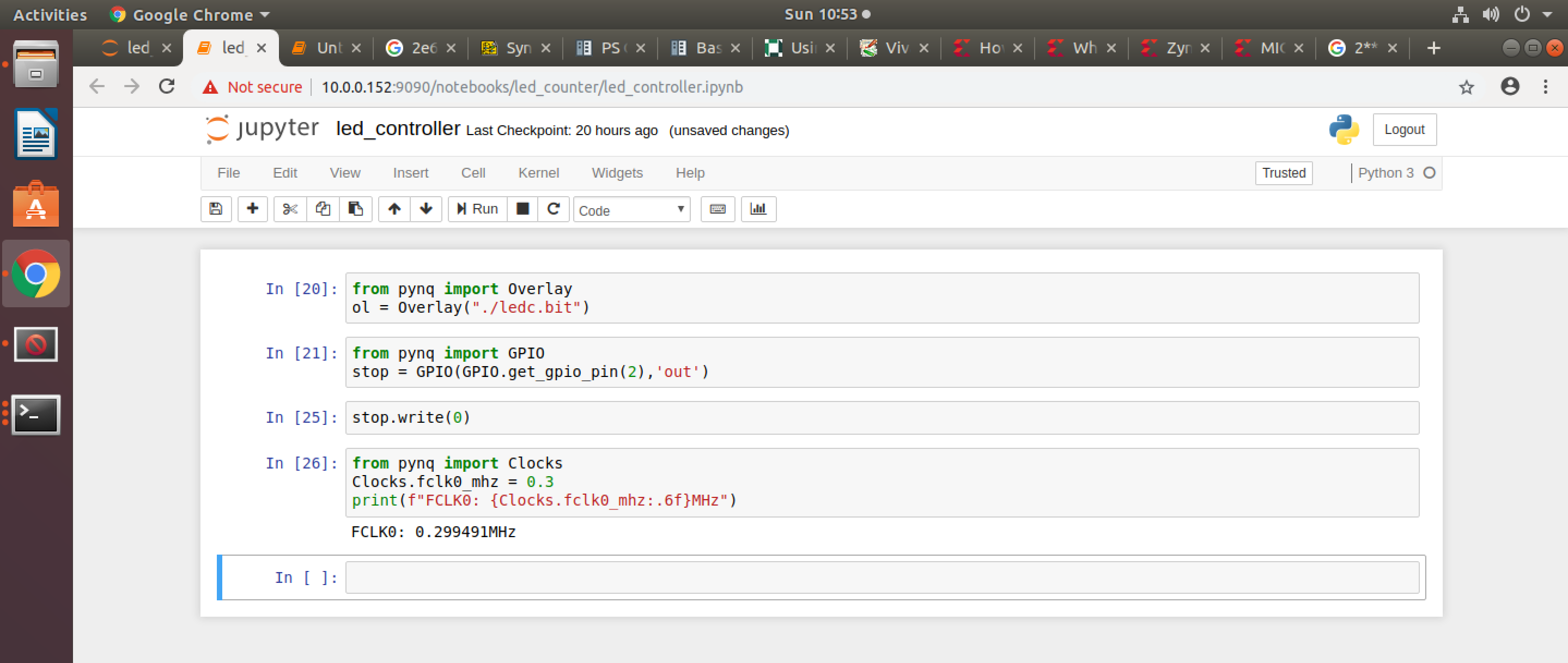
Assuming it is working now let's break out the Python side of our control. Taking advantage of the Zynq Python API to interface with the GPIO pins, I set pin 2 (remember we Sliced that one down to be our "stop") signal:
from pynq import GPIO
stop = GPIO(GPIO.get_gpio_pin(2),'out')
I next added a line to make sure the "stop" signal is off for right now.
stop.write(0)
If your LEDs are currently chasing/scrolling, go ahead and rerun that line with a 1 instead. It should stop things. Even if you press the two buttons it should remain stopped (because stop has the highest priority of all commands).
Set it back to 0 an then hopefully make it scroll again.
Finally we can change the frequency of our fabric clocks from Python. This is really nice since it can let you get some debugging capabilities without having to rebuild your file. I think in my video I'm running at 200 MHz. Note this cannot be arbitrarily set. You go too high it will crash/pull two much power. Also remember the design was built thinking the clock is at 50 MHz, so you're likely running the logic out of spec...for an LED chaser who cares, but if you're doing something important, weird stuff might happen.
from pynq import Clocks
Clocks.fclk0_mhz = 100 # or 200 or different values.
print(f"FCLK0: {Clocks.fclk0_mhz:.6f}MHz")
These lines of code should ensure a visible LED chase phenomenon based off of the button presses like shown in the video... If you'd like to turn off your LED chase, you can do it via Python!
stop.write(1)
Then to turn it back on (in my implementation anyways) I have to:
stop.write(0)
and then press either the left or right buttons that I designed.
OK... with this we're done! You should be able to interact directly with your Verilog code from Python and from your buttons to make a real-world change. This is really powerfull since it demonstrates a very basic way for information to go from your computational element (the Zynq Processor cores) down to a custom circuit living in the FPGA fabric.
There are more advanced and efficient means of sending data between these two environments which we'll cover in a future readthrough/lab thing, but for now we can just revel in this thing. Python has a lot of cool libraries...you could potentially have Python access online resources, scrape them, then send data down to the FPGA to be processed quickly, then send its result back up. Crazy.
As an extra bonus challenge, Feel free to return to your design and up some GPIO inputs on the PS (to read the buttons) if you want. GPIO API docs are here.
Show your working LED chaser to a staff member.

design_1.v file (the product of all the block diagramming) and your led_controller.sv file.
A few Things Moving Forward
Version Control of Projects
It would be good practice to try and run version control on your Vivado projects. This actually used to be really challenging since Vivado would intermix temporary build files with actual reference and source files so if you weren't careful your'd be version controlling raw binaries and things which just messes everything up. Since 2022/2023, they've largely reorganized how files are set up inside a project. If you go into your lab 1 project folder, you'll see a whole bunch of folders that are like "lab01.cache" or "lab01.gen", etc...Most of these
For version control, the two things you need to track should be:
- The
.xprfile which is the top-level summary of describing the project - The
.srcsfolder and everything in it.
Everything else can be regenerated from the contents of these two files/folders so when you are working with teammates and integrating code, try to only have your repo have this stuff! You may still have some nasty merges when it comes to things like IP...things that you may just have to pick one or the other rather than line-by-line merge, but it does prevent you from getting all messed up with all the temp files. This little summary here I think covers this pretty well. If you have some time, feel free to do this with the project you just made. Then make a new folder, clone the contents, open it up in Vivado, and you basically just need to regenerate the output products and rebuild.
Other Editors
The lab machines all have have VSCode (run code in a terminal) on them as well as vim and sublime. Feel free to use those rather than the Vivado editor. You can basically open any Vivado file from outside and edit it...the only caveat on this is do NOT have that file open inside the Vivado editor at the same time...it will notice that the file has been edited by something else, but often times will just happily fight back and undo your edits. So a completely respectible workflow could be to have Vivado open at the block diagram level, but you have VSCode or something actually opening up all the .sv files.
Take some time to explore all the files showing up in the .srcs folder. The files don't exactly exist in the most intuitive locations. Also always make sure that the files you're using are inside that folder and aren't symlinked out and/or referenced somewhere else in your computer (why we tell you to copy files into project when creating). Storage is cheap and it is much more manageable to just have all-together copies of files than things linking to one another. Especially when collaborating on projects with folks.
Lab initially inspired by video here