Pynq 02
Doing more...
Please Log In for full access to the web site.
Note that this link will take you to an external site (https://shimmer.mit.edu) to authenticate, and then you will be redirected back to this page.
A Simple Memory-Mapped Interface
In this lab we'll look at making a Memory-Mapped piece of IP on the PL and then access it from Python (the PS). This will be used to control the MAX7219 display. The performance won't be amazing, but also this display doesn't need great performance and it should demonstrate the overall pipeline and how we can build some simple Verilog which will then get implemented in the PL. We will wrap this module up so that it becomes AXI-interfaceable IP, which means we can then link it conveniently and scalably to our PS.
Getting Started
So, I'm assuming you already did the first lab with Pynq. We can skip a lot of "click here" steps, but of course refer back to that as needed.
Start by making a new project targeted for your PYNQ-Z2 board. Add the same constraint file as last week. When setting it up, make sure that you specify the Board File rather than just choose the correct chip.
Once you're in your new project, go to your xdc and comment out everything except the four leds, the four buttons, and three of the "Arduino GPIO" pins. We just need three and any three should work, but I used the three corresponding to BGA pins T14, U12, and U13. I named them cs, data, and clk, respectively.
create a new block diagram like before, and add a ZYNQ Processing System. Run the connection automation right away.
Remember to allow it to run the self-automation on the Zynq core!! This configures the clock frequency among other important things.
Add four output ports to correspond to the four things left in your xdc file:
csdataclk[3:0] leds[3:0] btns
Set up for AXI
What we want to do is create a memory-mapped interface that we can access from our Python environment. For this lab we will utilize one of General Purpose AXI Interfaces we've heard about in Lecture 03 from this past week. Specifically we'll use one of the PS Master AXI Ports.
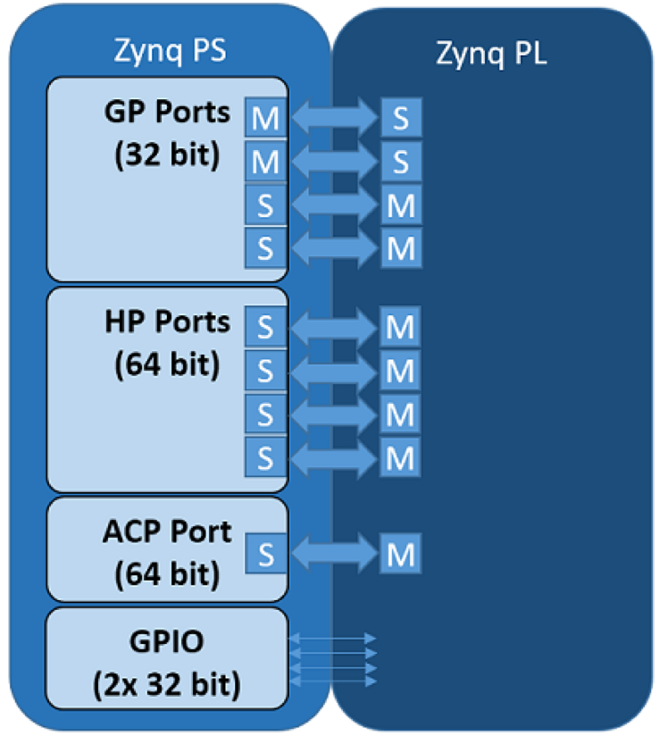
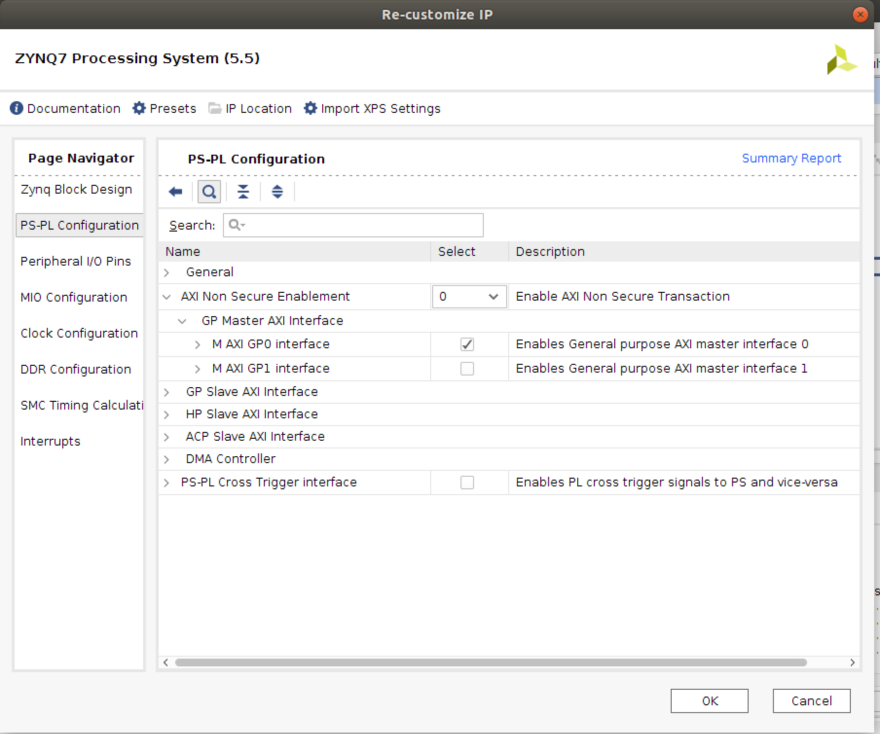
Chances are your Zynq processing system IP has already included that, but if it didn't open up your IP and then under the PS/PL tab, and under AXI Non Secure Enablement, ensure that a General Purpose AXI Master Interface (Pick GP0), is activated.
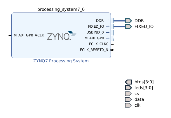
Afterwards (or maybe already automatically), your block diagram should look like the following:
Create a Piece of AXI IP
Now we need to build some IP that will interface with and AXI interface! Do the following:
- Go up to
Tools > Create and Package New IP - Click
Next - Select
Create AXI4 Peripheral - Call it whatever you want at the next window, and feel free to position the IP you're about to write anywhere in your file structure. I usually keep a pile in my home directory under a folder called
joes_ip, but that's just me. - In the next window that comes up it will show you a default module that has a single AXI4-LITE Slave Interface. That's in fact what we want here. We'll keep the defaults pretty much:
- The data width will stay at 32 bits (we can't change this actually since AXI-Lite requires 32 bits)
- Set the number of registers at 8. This will give you enough space to play with for the problem at hand.
- Click
Next - At the next window we're going to want to immediately go in and start editing our IP so click on
Edit IPwhich will now take us to our IP editor.
After you create your IP or if you ever need to edit it in the future, always feel free to right/control click on it in the block diagram view and then select Edit in IP Packager!
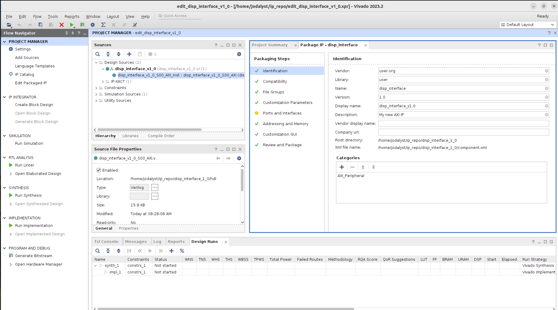
Once the IP editor is up, navigate into the sources menu and you will see a nested set of two Verilog files which represent your default AXI4-Lite Wrapper fitted to our specifications. Double click on the inner file (the outer one calls an instance of the inner one...the inner one is where the good stuff is at.) You'll note my IP is called disp_interface below (again you can name yours whatever, I'm just mentioning that for reference going forward).
This Verilog file, believe it or not, actually takes care of all the AXI-LITE timing and state machine handling for us! Study this file. The file has actually created a number of internal holding registers that have names like slv_reg0, slv_reg1, etc... These are each 32 bits in size and are the core of the data interfacing betwen the PL and PS in this example1.
CORRECTION
(Update 9/15/2024 ~@5pm): I don't know why I keep coming back to Xilinx. They keep breaking my heart. This lab works perfectly fine with Vivado 2023.2 and before. For whatever reason, Vivado upgraded their IP generation stuff in 2024.1 and it turns out the AXI-Lite interface they generate for us is broken. The wrapper is fine, but the inner file is borked and I'm still not 100% sure what is the issue. I ran a few tests and saw some differences, but nothing that should be game-changing. Nevertheless, Go into your inner verilog file and wipe all the code out. Instead replace that function with the code in this file here: good_axi_lite.v.
Few things to note, I made notations about where to put the changes discussed below (search for "joe" in the comments to find spots).
You may need to change the name of this module to match your hierarchy/IP construction.
OK so what should this module do? We've got eight 32 bit registers that we can use to exchange information between the PL and PS. We're going to use them roughly like so:
-
register 0 (
slv_reg0): this register will hold a hard-codeddeadbeefas a test value to read in Python -
register 1 (
slv_reg1): this register will hold the values of the four buttons to be read by Python (useful for inputs or debugging). -
register 2 (
slv_reg2): is used to specify whether we're doing a draw command (1) or configuration command (everything else) -
register 3 (
slv_reg3): contents to write.- If a configuration command, the
command_outshould get set to be this value stacked twice (so{slv_reg3,slv_reg3}. - If a draw command, the
command_outshould get set to a 64 bit command that uses these 32 bits to set the pixels in in the row specified in register 4 (below)
- If a configuration command, the
-
register 4 (
slv_reg4): second register for drawing. It will specify the row to be drawn to (refer to the MAX7219 datasheet for how to use these bits). -
register 5 (
slv_reg5): a trigger register. Nothing will actually get written or read here, but the act of writing to it by Python will be used to generate the trigger to run the SPI module.
Within both the inner and outer modules you should add the following inputs/and outputs (that will get interfaced to our SPI Controller):
  // Users to add ports here
  input wire [3:0] btn_in, //joe
  output wire [63:0] command_out, //joe
  output wire trigger_out, //joe
There's a few things to point out. The inner code as it exists is basically set up to let Python write to and read from the eight registers we created. If we want to break out their functionality to the module, you'll have to add stuff. We want to do a few changes additions in line with our stated goals
First we want to set some values to be readable in Python. That can be injected by changing the lines of code in the register read portion towards the bottom of the file. Specifically I modified that region like so:
	always @(*)
	begin
	      // Address decoding for reading registers
	      case ( axi_araddr[ADDR_LSB+OPT_MEM_ADDR_BITS:ADDR_LSB] )
	        3'h0   : reg_data_out <= slv_reg0; //replace with deadbeef (joe)
	        3'h1   : reg_data_out <= slv_reg1; //put button values into reg data
	        3'h2   : reg_data_out <= slv_reg2;
	        3'h3   : reg_data_out <= slv_reg3;
	        3'h4   : reg_data_out <= slv_reg4;
	        3'h5   : reg_data_out <= slv_reg5;
	        3'h6   : reg_data_out <= slv_reg6;
	        3'h7   : reg_data_out <= slv_reg7;
	        default : reg_data_out <= 0;
	      endcase
	end
A second thing we'd like to do is produce PL-side signals from register content. Since we're sending a 64-bit message to our SPI transmitter, we basically need to decide how to put stuff into that command out path that is correct. At the very end of the file is a region for user-added code. In that region I put something like this:
	//joe added code:
	reg [63:0] command;
	assign command_out = command;
	always @(*)begin
        if (slv_reg2==1)begin
	       command = {64'b0}; //change me
	   end else begin
	       command = {slv_reg3, slv_reg3};
	   end
	end
You should finish that.
The third thing we want to do is cause a trigger from Python (basically position data in our our comman_out line and then from Python trigger a write. There's several ways to do that, but one way you'll often see in MMIO systems is doing a write event to a particular address.
Further up in the page in the code region where PS-side writing is processed, I'm going to add this line (somewhere in the 210/220-ish range of the file):
trigger <= slv_reg_wren&&(axi_awaddr[ADDR_LSB+OPT_MEM_ADDR_BITS:ADDR_LSB]==5); //trigger when write happens to reg 5 (joe)
What this line does is basically set trigger to high when a write happens to register 5. It doesn't matter what is written, just that something is written. This is great, easy way to generate a trigger signal.
When you've made your changes (or what you think are changes), go to the Package IP tab and click through each option and make sure they are green (you may have a non-critical IO warning about AXI CLK speed...ignore). The last one will be "Package IP" or something. Go ahead and click and it'll take you back to you main project.
If you made errors building stuff here, you can always return to this by recustomizing this IP from your main block diagram window. If you needed to make any changes (now or in the future) to your IP module, you'll need to always need to make sure you go through the repackaging checkmarks. This is important since it'll tell you what needs to be automatically updated, etc. For example a change in the Verilog file will require you to refresh stuff in the File Groups tab, and you'll almost always have to go the final Review and Package tab at the bottom and click on Re-Package IP.
Assuming you've built everything and all is good (and you've packaged the IP), it will ask if you'd like to return to your project. Click OK. If it doesn't and all is saved, you can just exit the IP project (but not Vivado overall).
Upon exit, it may also pop up a window about Generating Output Products. If that comes up, make sure to click Global, and totally and feel free to click on Generate. (you'll need to do that now or in the future).
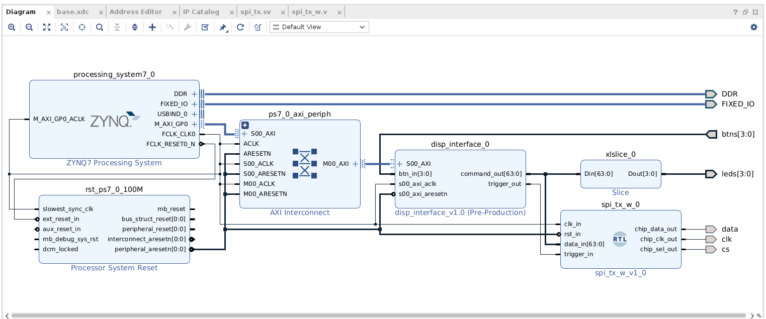
Back in Block Diagram
When back into the main block diagram, add an instance of your new module. You should be able to just search for it by name under your IP entry field. (Mine was named disp_interface)
You should be prompted to allow the system to automate the AXI wiring. Click on that and let it do its thing:
I'd now add in your validated SPI TX that your wrote previously. Make a wrapper for your spi_tx just like before. Make sure it is verilog. One thing I did here is bury/hide the busy_out signal since we won't be using it. Also I made sure to invert the resest signal since the reset signal used globally with AXI is active low, but our reset is active high. This let's our spi module use the global reset.
module spi_tx_w(
     input wire clk_in,
     input wire rst_in,
     input wire [63:0] data_in,
     input wire trigger_in,
     output wire chip_data_out,
     output wire chip_clk_out,
     output wire chip_sel_out
    );
    spi_tx  #(.DATA_WIDTH(64), .DATA_CLK_PERIOD(20))
    mspi
    (   .clk_in(clk_in),
        .rst_in(~rst_in), //IMPOTANT!!!
        .data_in(data_in),
        .trigger_in(trigger_in),
        .chip_data_out(chip_data_out),
        .chip_clk_out(chip_clk_out),
        .chip_sel_out(chip_sel_out));
endmodule
Add that module into your project and connect everything up. Notice I sliced the bottom four bits off of the command bus and put them on the led's to help with some debugging. If you haven't already let Vivado automatically wire the AXI stuff up for you. Note it isn't smart enough to wire up your modules like data_clk etc... so you'll have to do that yourself. When done you should have something like this:
Depending on the order of operations from before you may get prompted about generating output products here (if you didn't earlier). The window looks like the following. It is very important that you make sure Global is specified~
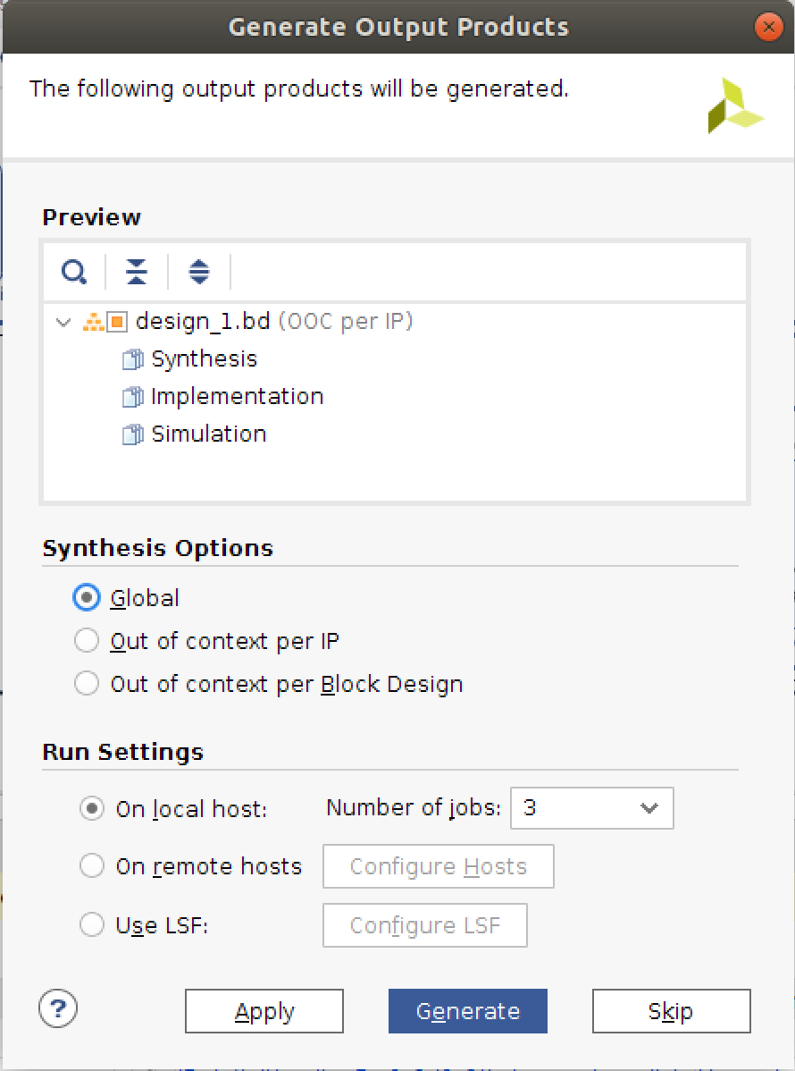
Just to reiterate, make sure to specify Global under Synthesis Options when it pops up. If you don't you'll get errors/critical warnings related to Out of Context Build issues later on. If you forgot to do this or can't remember you can always right click on your block diagram, go to Generate Output Products, change things and then click Generate.
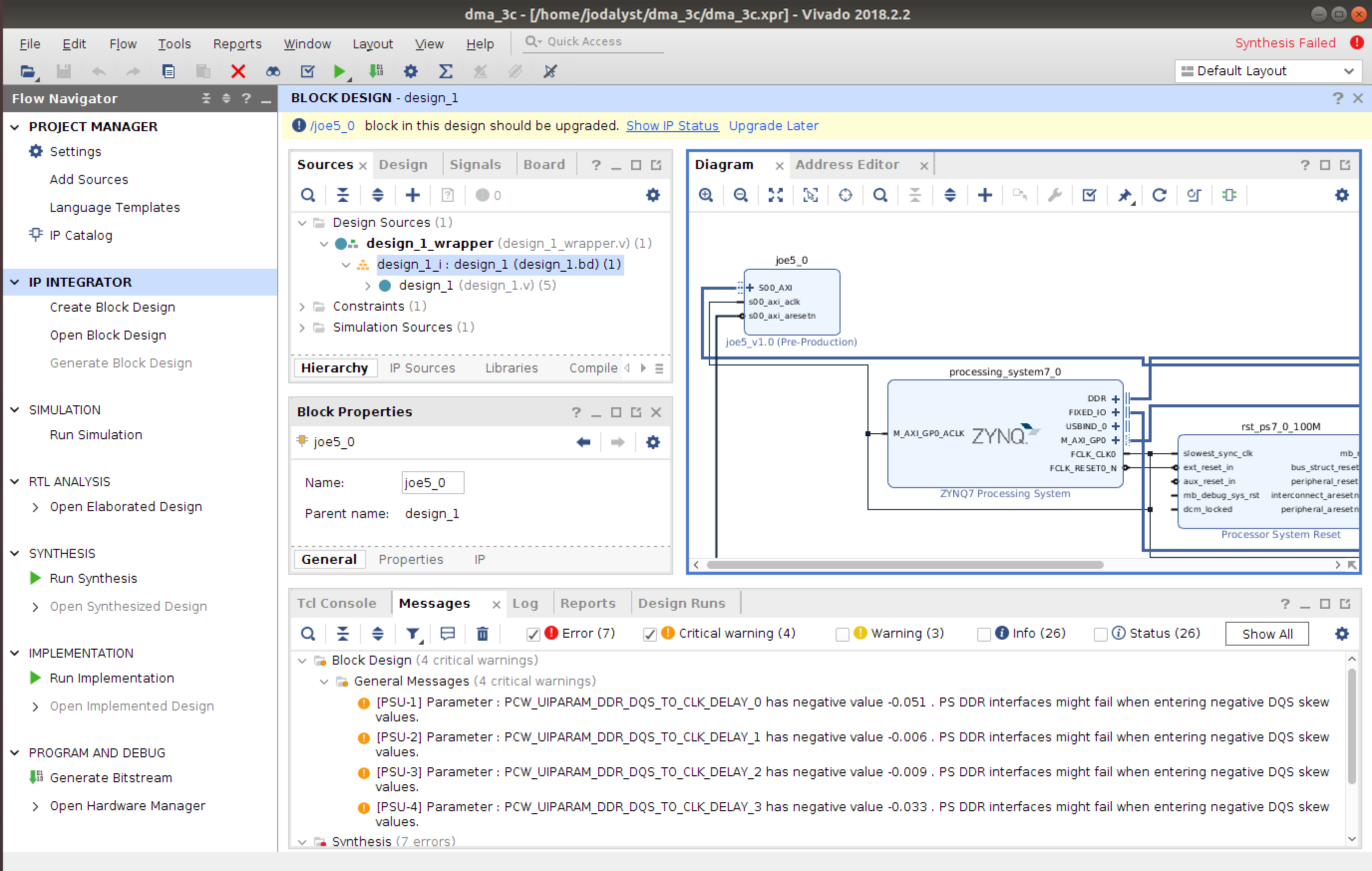
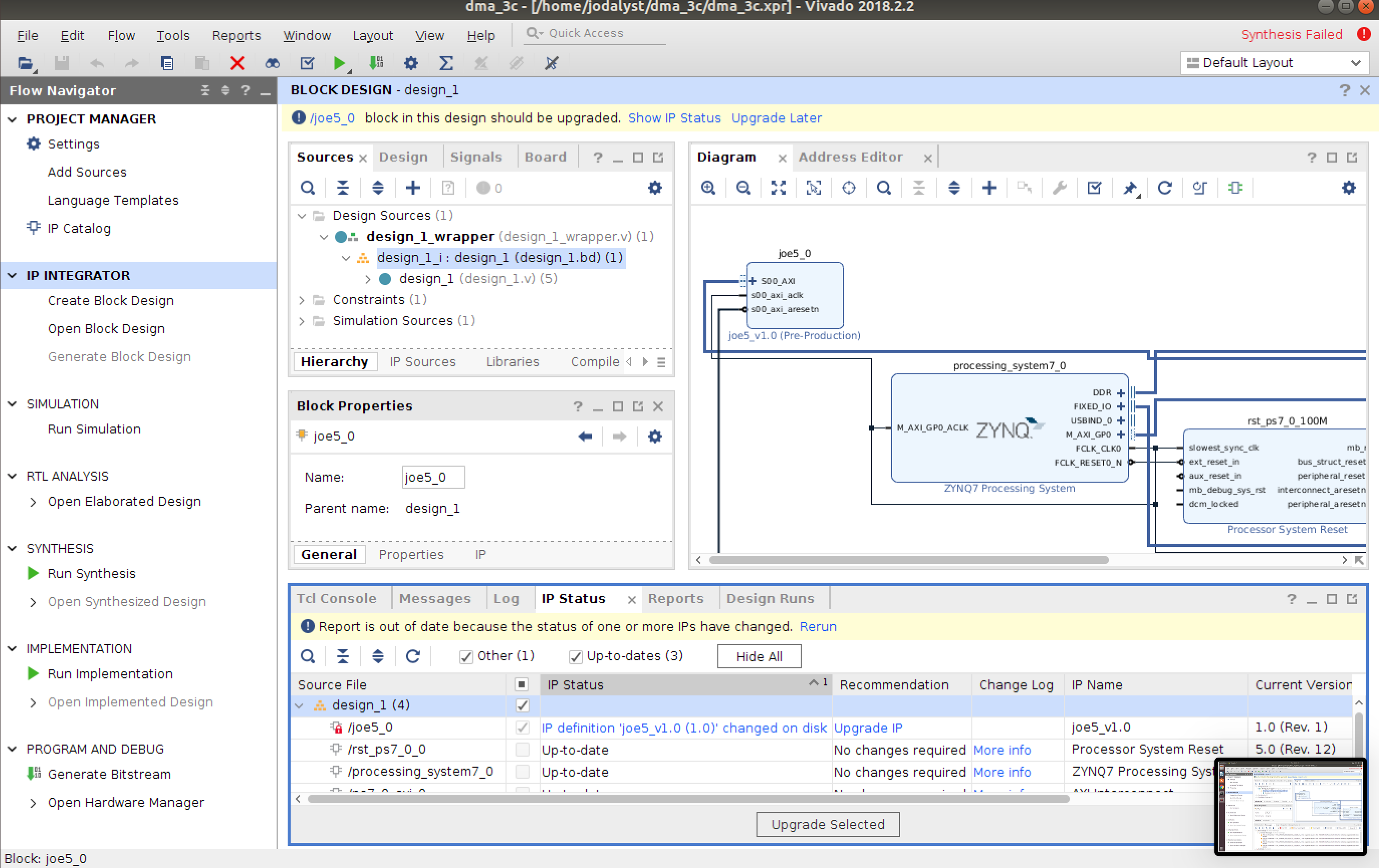
You are always free to go back and edit IP and stuff in the future, just remember at every step along the way just regenerate things (make sure Verilog is refreshed, saved, etc). Also note that if you go and update your IP at any point after having integrated it, Vivado will notice and prompt you to update/refresh all your IP. That will usually come up as an error, or a more friendly yellow notifier at the top. See the two images below:
Back on our main plot-line here, if all is good, verify your block diagram with the check-mark symbol.
Then right-click on your block diagram file, and go to Create HDL wrapper. If that builds fine, then save everything, and go to Generate Bitstream. AFter that is completed (hopefully with no errors).
Interacting with it in Python
Ok deep breath...now hopefully things are maybe working...oh goodness.
Get your bitfile and hwh file up to your notebook. Make the new notebook and bring it in like we did last time:
from pynq import PL
PL.reset()
from pynq import Overlay  #import the overlay module
ol = Overlay('./design_1.bit')  #locate/point to the bit file
Assuming that loaded fine, let's do a thing we skipped last week. Run these two lines:
import pprint
pprint.pprint(ol.ip_dict)
What should pop out will be a massive dictionary that is basically the device tree of everything within your project. This is what that hwh (hardware handoff file) has been doing for us these last few times...giving the info to the pynq framework about what it needs. When I look at my stuff, I'll see a device labeled disp_interface_0 which is related to the name of my IP. I can access that piece of MM IP just by doing ol.disp_interface_0.
Then going into the Pynq docs, I can interact with this piece of IP using very basic commands like read and write while providing data. Try this simple script here. It writes some values to your registers and reads others. You should see some green LEDs light up on your board. You should also see data from those registers. One should be the hard-coded deadbeef, the other should be based on the four buttons you're pushing...make sure torun a few times with different button states to see what happens.
j5 = ol.disp_interface_0  #find the AXI MMIO module which we can talk to (name of IP)
#Now it is time to interface with the j5 IP:
j5.write(0x08,0)  #write 0 to address location 0x08 (command type)
j5.write(0x0C,5) #write "5" to address location 0x0C (should show up on green LEDs)
j5.write(0x10,2) #write 2 to address location 0x10
d = j5.read(0x04)  # should read the value of all four push buttons (for test)
print(d)    #print output (hopefully buttons)
d = j5.read(0x00)  # read deadbeef hopefully (hard-coded in your mmio)
print(hex(d))
Now let's interact with the SPI controller. We set register 0 to 0, then send commands and write to the trigger register. When done the display should be ready to write to!
j5.write(0x08,0)  #write 4 to address location 0x00 (command type)
j5.write(0x0C,0x0F000F00) #display test command
j5.write(0x14,0x0) #trigger
j5.write(0x0C,0x0C000C00) #turn off display
j5.write(0x14,0x0) #trigger
j5.write(0x0C,0x0C010C01) #display on command
j5.write(0x14,0x0) #trigger
j5.write(0x0C,0x09000900) # decode mode 0
j5.write(0x14,0x0) #trigger
j5.write(0x0C,0x0B070B07) #scan mode command
j5.write(0x14,0x0) # trigger
j5.write(0x0C,0x0A010A01) #screen intensity set
j5.write(0x14,0x0) #trigger
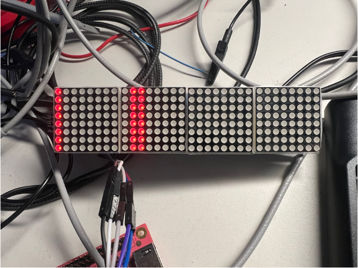
The display hopefully flashed or at least dimmed a bit when the config commands were getting written. Now let's draw. The following example code will write three vertical lines on the screen:
j5.write(0x08,1)  #write 1 to address location 0x00 (drawtype)
for y in range(1,9):
    j5.write(0x10,y)  #write y to address location 0x08 (row address y indexed)
    j5.write(0x0C,0x00000601)
    j5.write(0x14,0x0) #trigger
If it ran fine, you'll get a pattern like this:
If not...well better head back to the design and figure out what went wrong. One thing you may want to do is make sure you are actually triggering SPI writes. A logic analyzer or an oscilloscope may be helpful here.
Eventually you'll get it working though. I believe in you. This is getting sweet...you can smell the layers of abstraction piling up. And they smell good. In the field (or your final project), you could now imagine that you could perform a complex operation in the hardware quickly (let's say a Fourier Transform on some audio data, and then extract certain peaks and report them back, and have all of that wrapped up in a nice little function that anyone could use.)
Finishing Up
Do something with the display. Make an animation or a game or something. You have access to the buttons via register 7, so you can take user inputs. Or make an animation. You're doing all this in Python, so I don't want to hear any complaining. Programming won't get any easier than that until AI takes all our jobs.
Lab initially inspired by video here
.v file (the product of all the block diagramming),file.

Footnotes
1remember in lecture how I said Xilinx/AMD really use Master/Slave terminology a lot...this is another example of that. All the auto-generated stuff doesn't even just use M/S prefixing but "slv" as you can see. Hence, we'll just roll with it to avoid adding an extra layer of confusion on us.